Executive Summary
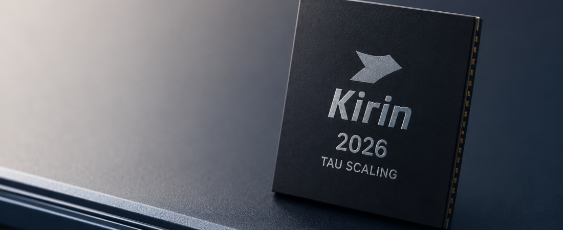
According to the available source information, Huawei’s upcoming Mate 90 smartphone series has entered chip packaging and testing and is being prepared for a reported September 2026 launch. The device is expected to debut Huawei’s new Kirin 2026 processor, which the report says incorporates the company’s proprietary “Tau Scaling” concept as part of a post-Moore semiconductor strategy.
On the surface, this is a handset launch story. Strategically, it may be more important as a signal about how one of China’s most closely watched technology companies is trying to operate under long-running semiconductor constraints. Rather than framing progress around access to the most advanced process nodes alone, the reported positioning around Tau Scaling suggests a broader emphasis on architecture, integration, and packaging.
That distinction matters for Asia’s semiconductor landscape. If Huawei is formalizing a design approach meant to extract more value from system-level engineering, it could reinforce the importance of domestic capabilities beyond wafer fabrication, including packaging, testing, and the wider chip supply chain. At the same time, the available information does not yet establish how the Kirin 2026 is built, how it performs, or whether the approach can scale efficiently.
For investors and industry observers, the key takeaway is not that Huawei has already solved China’s advanced-chip challenge. It is that the company appears to be advancing a practical response to it. Whether that response is commercially and technically durable remains the central question.
Watch the Short Brief
This short explains why Huawei’s reported Kirin 2026 debut may matter more as a post-Moore semiconductor strategy signal than as a smartphone launch.
Key Developments
According to the source summary, Huawei’s Mate 90 smartphone series has moved into the chip packaging and testing stage. The same report says the phone line is targeted for a September 2026 launch window.
The headline development is the planned debut of the Kirin 2026 processor. The available source information describes the chip as using Huawei’s proprietary “Tau Scaling” concept, represented by the Greek letter τ, within a post-Moore strategy.
Beyond that, the confirmed details remain limited. The available information does not specify the processor’s node, performance targets, power characteristics, foundry arrangement, or packaging and testing partners. It also does not explain the technical mechanics of Tau Scaling in detail. That means the current significance lies less in verified specifications and more in what Huawei’s reported positioning may indicate about its broader semiconductor direction.
The broader context is clearer. Huawei has operated for years under US-led technology restrictions that have affected access to parts of the global advanced semiconductor ecosystem, including leading-edge manufacturing equipment. In that environment, any reported effort to define a proprietary post-Moore framework is notable because it points to adaptation rather than simple delay.
The packaging-and-testing milestone is also important in practical terms. It suggests the product is moving toward production readiness, even if the final timing and scale of launch still need to be validated by the market.
Strategic Analysis
The semiconductor industry is no longer driven by transistor scaling alone. Across Asia and globally, performance gains increasingly depend on a wider stack that includes architecture, packaging, interconnects, software optimization, and power management. In that sense, Huawei’s reported use of Tau Scaling fits a broader industry direction. What makes this case distinctive is the strategic pressure behind it.
For companies with normal access to the global semiconductor supply chain, advanced packaging and system-level optimization are additional performance levers. For Huawei, according to the strategic context reflected in the draft and source framing, they may be closer to a necessity. That is why the reported arrival of Kirin 2026 matters beyond the smartphone itself.
One implication is that Huawei may be trying to define a post-Moore operating model suited to China’s current constraints. If accurate, Tau Scaling is not just a product label. It may represent an effort to organize engineering choices around what is still achievable without full access to the most advanced global manufacturing path. That does not by itself prove technical parity with leading international competitors. But it could suggest a more disciplined approach to extracting usable performance from a constrained environment.
This is strategically relevant for China’s semiconductor ecosystem. Much of the public debate around chip competition still centers on node leadership. That remains important, especially for AI accelerators and the highest-performance logic. But for consumer electronics and some broader compute applications, design integration and packaging can materially affect user experience even when process technology is not at the frontier. If Huawei can keep flagship products credible through those methods, it may strengthen confidence in a wider industrial path that depends on more than leading-edge lithography alone.
That possibility is especially important in Asia, where semiconductor competitiveness is distributed across multiple layers of the value chain. Foundries matter, but so do assembly, packaging, testing, substrates, materials, equipment, and system design. A Huawei strategy that emphasizes post-Moore execution could draw more attention to those adjacent layers within China’s domestic stack and across regional supply networks.
Still, the unknowns are substantial.
First, the technical meaning of Tau Scaling is not yet clear from the available information. It may involve architectural choices, packaging decisions, or system-level optimization, but the report summary does not define the implementation. Until Huawei discloses more, or third-party analysis becomes available, the term should be treated as a strategic signal rather than a fully understood technology framework.
Second, supply-chain capacity remains an open question. Advanced packaging is not a simple workaround. It can shift the bottleneck rather than remove it. High-end packaging and test flows require precision equipment, sophisticated materials, reliable yields, and strong process control. Even if the Kirin 2026 reaches market on schedule, the more important test may be whether production can scale efficiently and consistently.
Third, competitiveness is still hypothetical. The reported development may indicate progress, but it does not yet establish where the Kirin 2026 sits on performance, energy efficiency, thermal behavior, or cost. Those variables will determine whether Tau Scaling is mainly a branding framework, a meaningful technical advance, or something in between.
There is also a geopolitical angle. Export controls have often been discussed as a way to cap China’s chip capabilities by limiting access to the most advanced tools. A reported Huawei move toward a named post-Moore strategy does not invalidate that logic. The gap between access and restriction remains real. But it may suggest that the effects of containment are more complex than a simple freeze in capability. Companies under constraint may redirect effort into different parts of the stack, especially where system integration can offset some manufacturing disadvantages.
That is why this development deserves attention from policymakers as well as investors. If post-Moore approaches become more credible in China, future pressure points in the technology competition may increasingly include packaging, testing, design tools, and critical materials, not only front-end lithography.
Investor Takeaway
For investors, the most useful way to read the reported Mate 90 and Kirin 2026 development is as an indicator of where value and risk may be shifting inside China’s semiconductor strategy.
The immediate question is execution. Investors should monitor whether the reported September 2026 launch window holds, whether Huawei provides any concrete technical disclosure around Tau Scaling, and whether early product analysis supports the idea that system-level engineering is doing meaningful work. Independent benchmarks, teardowns, and supply-chain commentary will matter more than marketing language.
The second question is ecosystem depth. If Huawei’s approach proves viable at commercial scale, even in a limited sense, it could support the strategic relevance of packaging and test capabilities within China’s domestic semiconductor chain. That would not mean the country has closed the gap at the leading edge. It would mean more of the competitive story is moving into integration and manufacturing stages that sit beyond wafer fabrication alone.
The third question is cost. Advanced packaging and integration can improve outcomes, but they can also add complexity. If the Kirin 2026 relies on a more elaborate production path, investors will need to watch whether the benefits justify the manufacturing burden. Yield stability, unit economics, and production consistency could matter as much as raw benchmark performance.
Finally, there is a policy dimension. A credible Huawei launch built around a post-Moore narrative could intensify debate over whether current restrictions are simply delaying capability or redirecting it. That may not produce immediate policy changes, but it could shape where regulators and industry participants focus next.
At this stage, the reported Kirin 2026 should be viewed less as proof of a solved problem and more as a live test case. The strategic significance lies in Huawei’s apparent attempt to turn constraint into design doctrine. The market significance will depend on whether that doctrine translates into repeatable product performance, production reliability, and broader ecosystem support.