Latest posts
-
Samsung’s Reported Use of TSMC 3nm for Nvidia HBM Base Die Signals a New AI Supply-Chain Pattern
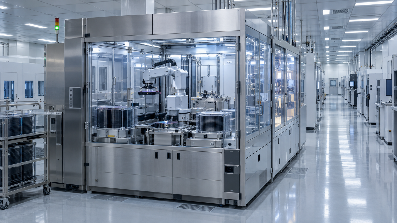
Samsung may be entering Nvidia’s HBM supply chain through TSMC, not against it. If confirmed, the move suggests AI memory is becoming more modular and less vertically integrated.
-
Mature Nodes, New Chokepoints: What the Reported TSMC-GlobalFoundries Interposer Deal Signals for AI Packaging and China
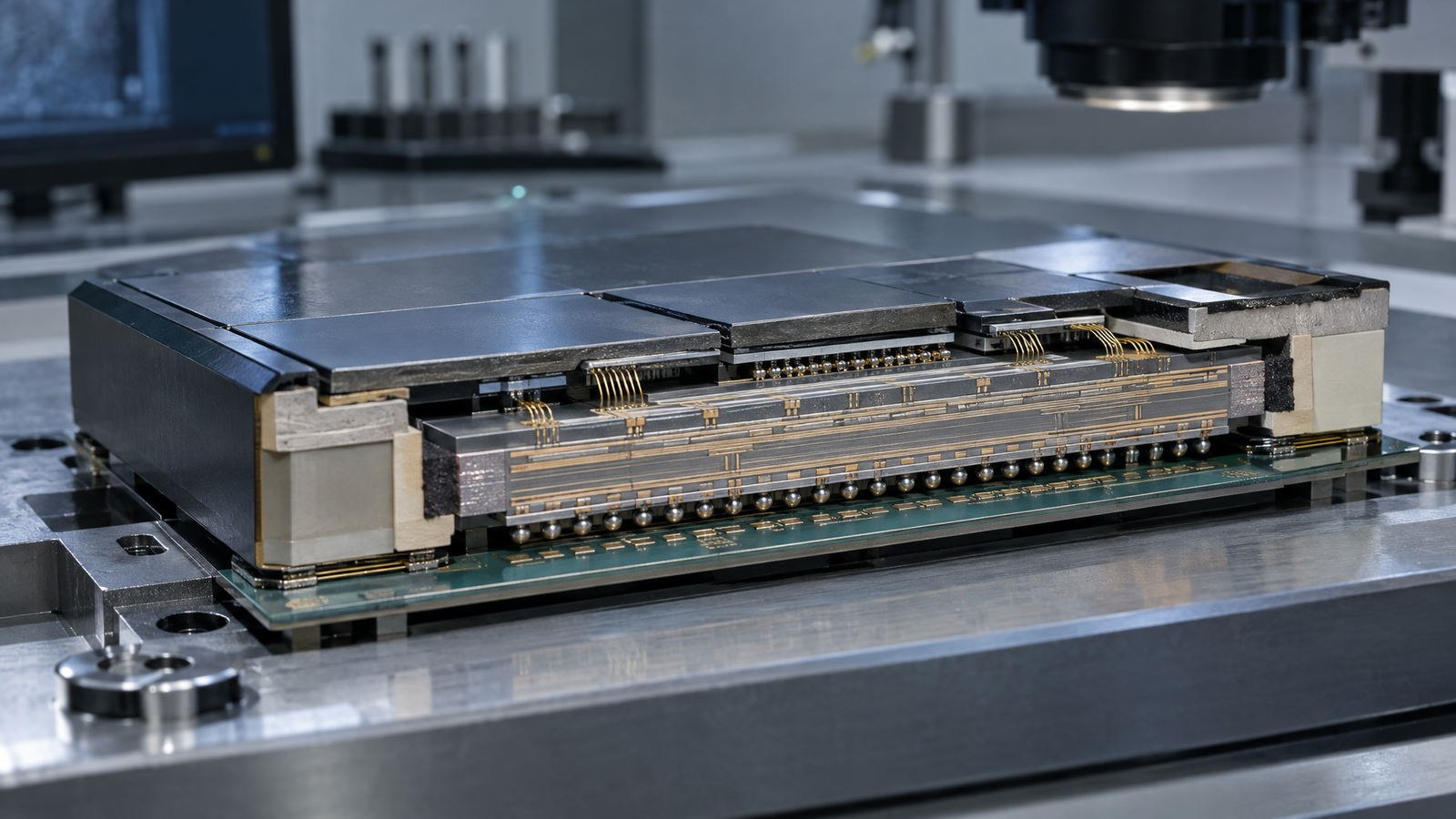
The reported TSMC-GlobalFoundries interposer deal suggests mature-node packaging inputs could become a critical AI chokepoint. That could lift the strategic value of legacy fabs while shifting supply-chain and geopolitical risk deeper into the packaging stack.
-
Japan Backs TSMC’s 3nm Kumamoto Expansion With Potential $4.1 Billion Subsidy Support
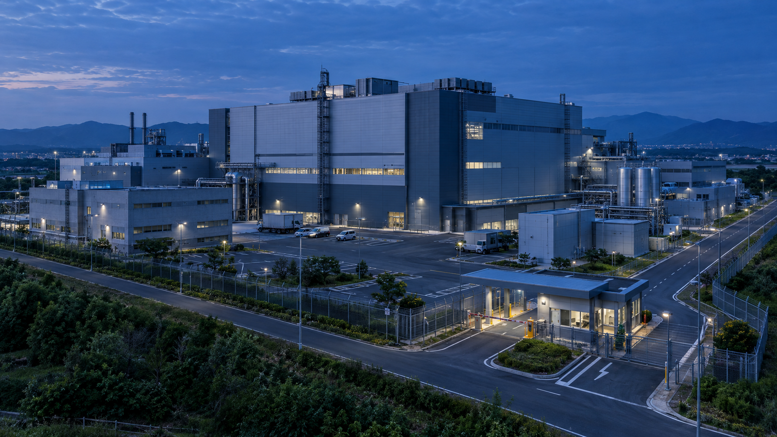
Japan’s approval of TSMC’s reported 3nm Kumamoto expansion is a strategic signal that advanced semiconductor capacity in Asia is increasingly being shaped by state-backed capital support.
-
AI-Defined Fabs: Nvidia and Semiconductor Leaders Push AI Into Chip Design and Manufacturing
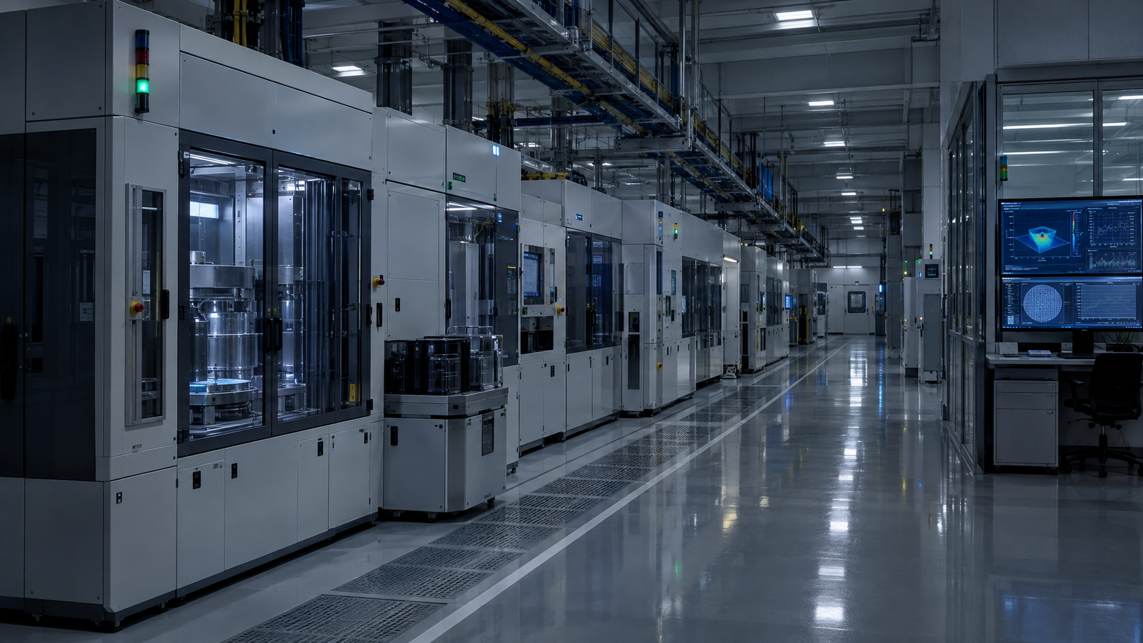
Nvidia’s latest collaboration signals a push to bring AI deeper into semiconductor design and manufacturing workflows. The key question is whether those tools can prove themselves inside East Asia’s real fabs.
-
TSMC’s Record Q3 Profit Highlights Taiwan’s Central Role in the AI Compute Supply Chain
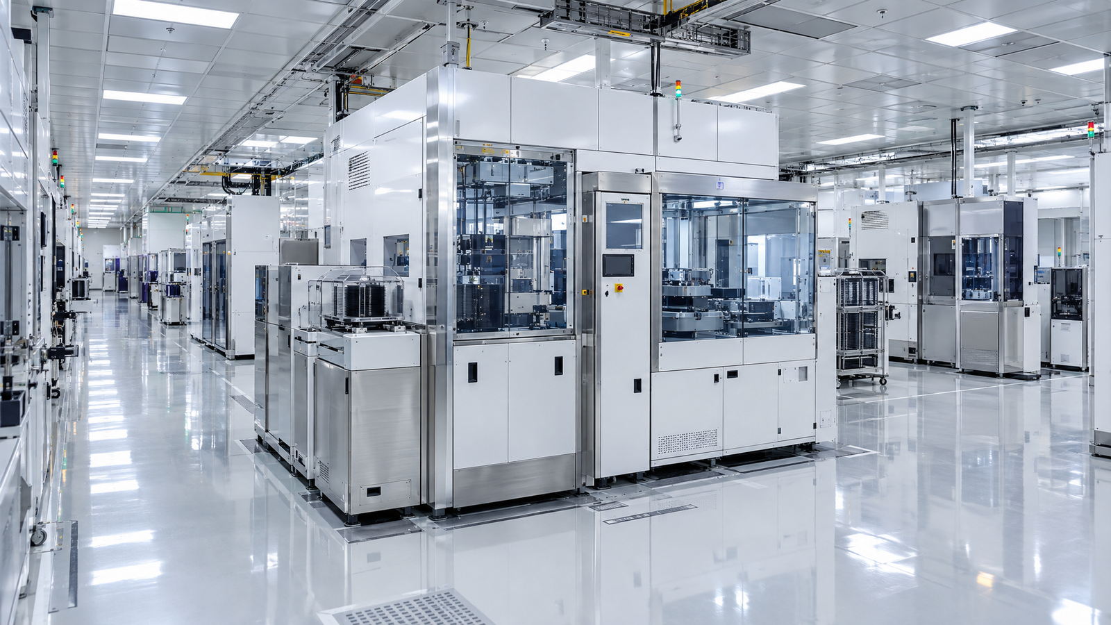
TSMC’s record quarter suggests AI demand is translating into real advanced-node manufacturing output, not just earnings momentum. The result reinforces Taiwan’s strategic importance and the concentration risk in the global AI hardware stack.
-
KYEC’s Nvidia Advance Payment Deal Signals a New Phase in US Backend Chip Capacity Buildout
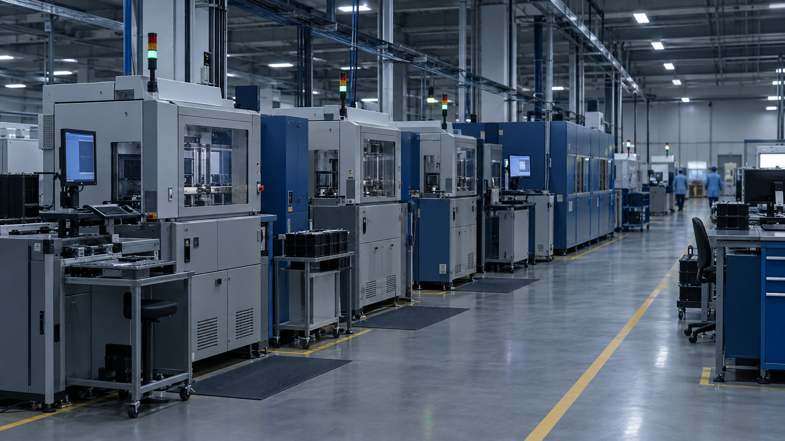
Nvidia’s reported advance payment to KYEC suggests backend chip testing is moving closer to the center of AI supply-chain strategy. The deal points to deeper supply pressure in semiconductor operations and continued Taiwanese OSAT relevance.
-
Beyond the Shrink: TSMC, Intel, and Samsung Turn to Early Equipment Integration for AI Chips
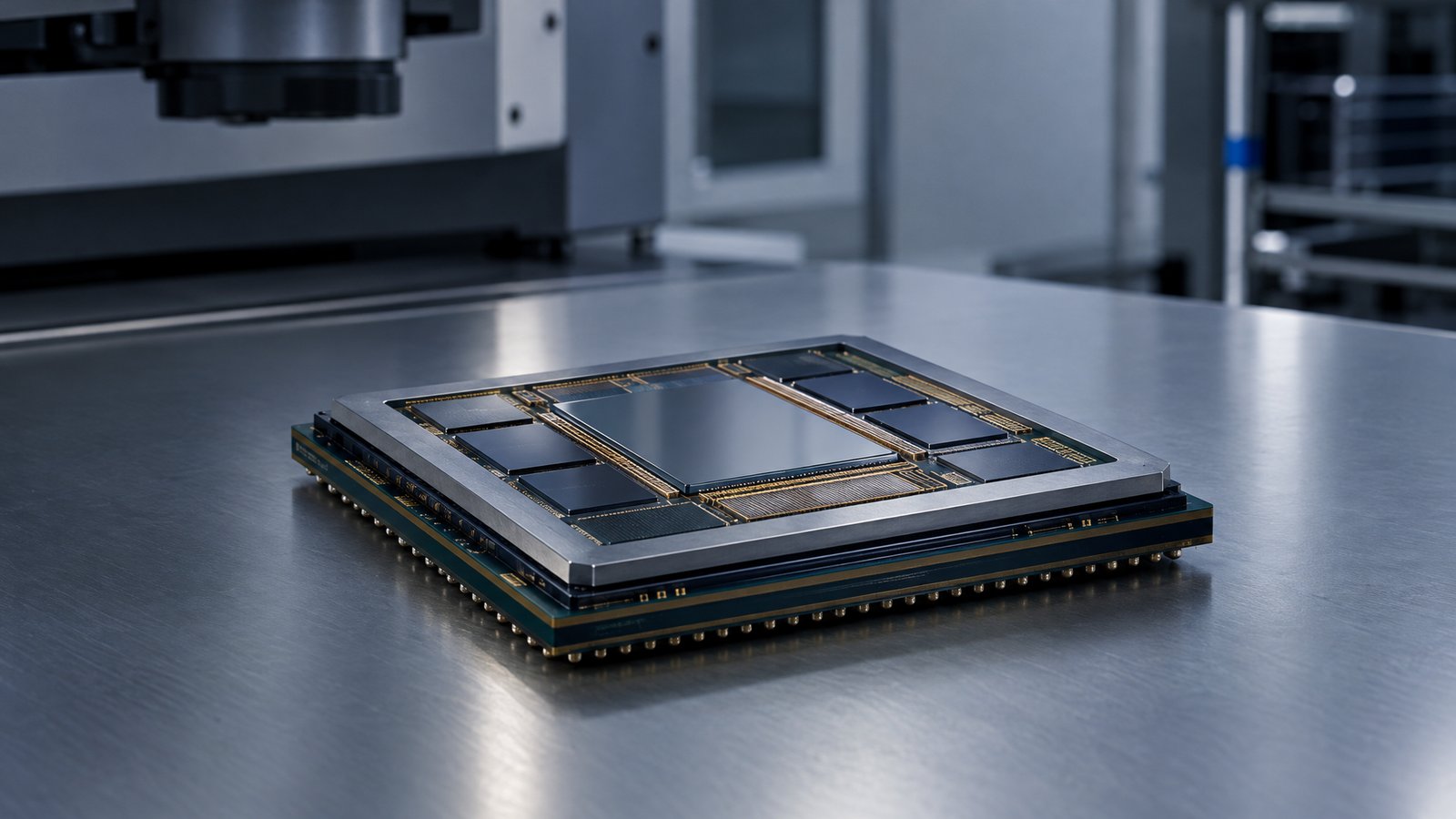
AI chip leadership may be moving beyond transistor scaling alone. Reported alignment among TSMC, Intel, Samsung, and Applied Materials points to earlier co-optimization in packaging, architecture, and manufacturability.
-
Microsoft’s Surface Launch Highlights Memory Cost Pressure in Local AI PCs

Microsoft’s latest Surface launch points to memory pricing as a key constraint on local AI PCs. The result could be a slower path from premium showcase devices to broader adoption.
-
CXMT’s Reported DRAM Progress Adds Pressure to Korean Memory Leaders

Samsung and SK Hynix fell after reported DRAM progress from CXMT, even though parity in yields, scale, and market share is not confirmed. The move reflects a shift in investor perception around future Korean memory leadership.
-
TSMC’s Record Q3 Revenue Points to Deeper AI Dependence on Taiwan’s Advanced Foundry Capacity
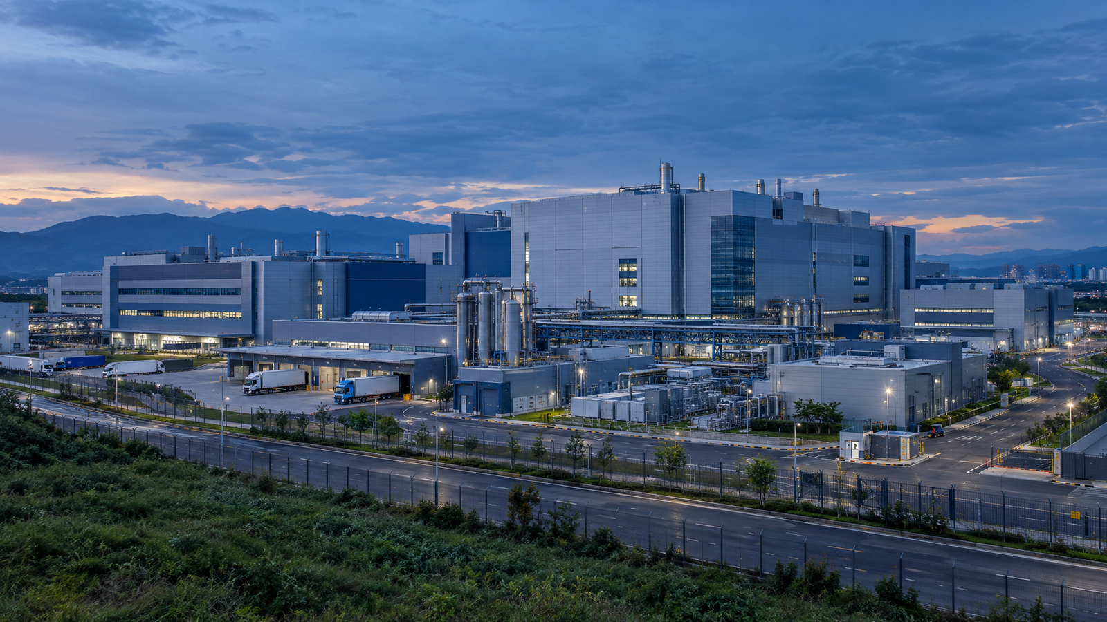
TSMC’s reported record quarter suggests the next phase of AI value creation may depend less on chip design alone and more on who can manufacture frontier chips at scale. The move underscores Taiwan’s central role in the AI infrastructure cycle.