Executive Summary
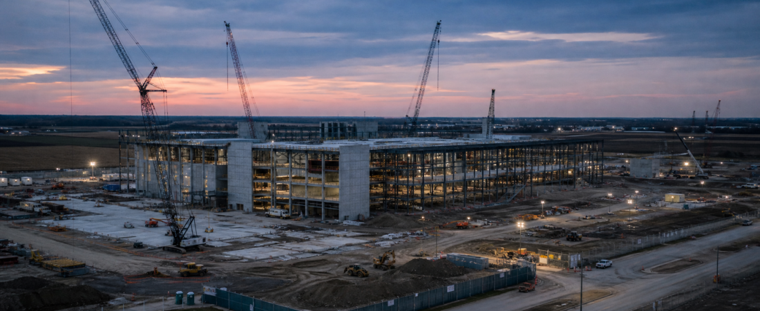
SK hynix has held a groundbreaking ceremony for a new advanced packaging facility in West Lafayette, Indiana, according to the available source information. The project is described as a $4 billion investment, with the plant’s cleanroom scheduled to open by October 2028 and mass production of next-generation high-bandwidth memory, or HBM, targeted for the second half of 2029.
For the AI hardware market, the announcement matters less as a near-term supply event and more as a long-duration signal about where critical semiconductor capabilities may be located in the future. HBM is a core component in modern AI accelerator systems, and advanced packaging is one of the most technically demanding parts of that value chain. Establishing that capability in the United States could gradually diversify a manufacturing step that has historically been concentrated in Asia.
For TechPowerAsia readers, the strategic significance sits at the intersection of semiconductors, AI infrastructure, and cross-border industrial strategy. The reported project suggests that a leading South Korean memory producer is extending its operational footprint closer to the US market at a time when AI supply chains are under heavier commercial and geopolitical scrutiny.
The timeline also matters. Even if the project progresses on schedule, its impact on current HBM tightness would likely be limited for several more years. That makes this development more important as a marker of future supply-chain direction than as an immediate answer to present-day AI hardware constraints.
Watch the Short Brief
Watch this short visual briefing for the key strategic implications behind the story.
Key Developments
SK hynix has broken ground on an advanced packaging facility in West Lafayette, Indiana, according to the source summary and company announcement referenced in the source material.
The reported investment size is $4 billion. Based on the available information, the facility is intended to support production of next-generation HBM, a memory category closely tied to AI accelerator demand.
The project’s reported operating milestones are long-dated. The cleanroom is scheduled to open by October 2028, while mass production is targeted for the second half of 2029.
The available source information links the project to a broader US-South Korea technology narrative. That framing comes most directly from SK hynix’s own announcement language rather than from detailed policy disclosures in the material provided. No specific government incentive package, subsidy structure, or formal bilateral mechanism is detailed in the source summary.
Nvidia appears in the related-company set for this story, but the available information does not confirm any supply agreement, output commitment, or customer-specific arrangement tied to the Indiana facility. The relevance is strategic rather than transactional: HBM is essential to the broader AI accelerator ecosystem in which Nvidia is a major end-market driver.
Strategic Analysis
The most important point is that this appears to be an advanced packaging investment, not simply an incremental memory capacity announcement. In the AI semiconductor stack, the performance and availability of HBM depend not only on memory fabrication but also on the ability to package and integrate those components into systems that can be deployed at scale. That makes packaging capacity an increasingly consequential strategic chokepoint.
From an Asia technology intelligence perspective, the Indiana project may indicate how leading regional chipmakers are adapting to a changed operating environment. South Korea remains central to the global memory industry, but customer concentration, supply-chain resilience concerns, and geopolitical pressure are all pushing manufacturers to reconsider where later-stage production steps should occur. A US-based advanced packaging site could be read as part of that broader geographic diversification.
That does not mean the industry’s center of gravity is shifting out of Asia in any simple way. Core semiconductor capabilities across memory, foundry, substrates, tools, and materials remain deeply anchored across Asian markets. But one strategic implication of the Indiana facility is that some of the most sensitive and highest-priority parts of the AI hardware chain may increasingly be distributed across allied manufacturing bases rather than kept as tightly clustered as they were in earlier cycles.
This is especially relevant for HBM because AI demand has changed the economics of the memory market. In prior periods, memory expansions were often discussed primarily through cyclical pricing and capacity utilization. HBM introduces a more strategic layer. It is tied to a specific compute buildout, requires more complex integration, and sits closer to the performance envelope of the end system. As a result, location decisions around HBM-related manufacturing may now carry greater geopolitical weight than traditional commodity memory expansions.
The US location also merits attention beyond symbolism. For SK hynix, building in Indiana may offer several strategic advantages if execution stays on track: closer proximity to parts of the US AI and semiconductor ecosystem, a more diversified operational footprint, and potentially stronger positioning in conversations around resilient supply chains. None of that guarantees commercial success, but it suggests the project is best interpreted as a structural positioning move rather than a short-term output expansion.
The project may also matter for how the market thinks about supply-chain timing. Semiconductor packaging capacity cannot be relocated or replicated quickly, especially for advanced AI-related applications. The reported schedule of cleanroom opening in 2028 and production in the second half of 2029 underscores that meaningful capacity additions remain multi-year undertakings. In practical terms, this means near-term HBM availability will still depend largely on existing facilities and current execution from incumbent suppliers.
Nvidia’s indirect relevance strengthens the market importance of the announcement without turning it into a customer story. Because Nvidia’s AI accelerators are among the products most closely associated with HBM demand, any future expansion in HBM packaging capacity could affect the resilience of the broader AI compute supply chain. But the available source information does not support drawing a straight line from this plant to a specific Nvidia production plan, allocation commitment, or revenue implication. The appropriate reading is that the facility may become relevant to major AI chip ecosystems, not that those relationships are already contractually defined.
There is also a longer-term strategic question embedded in this development: whether advanced packaging will become one of the main battlegrounds for semiconductor localization policy. Logic fabrication has historically attracted the most policy attention, but AI infrastructure places more emphasis on the integration of memory, compute, and packaging. If that trend continues, projects like this one could be seen as early evidence that advanced packaging is moving toward the center of industrial strategy, not just manufacturing execution.
Investor Takeaway
Investors should view the Indiana project as a long-horizon strategic development rather than a near-term earnings or supply catalyst. The reported timeline places meaningful production several years away, which limits its immediate effect on current HBM market tightness.
The first point to monitor is execution discipline. Large semiconductor projects are complex, and the gap between groundbreaking and volume production is where cost, schedule, labor, and tool-installation risks typically emerge. Progress toward the stated cleanroom milestone in 2028 will be an important indicator of whether the project remains on track.
The second is commercial visibility. The available information establishes the strategic relevance of the facility, but not the customer structure behind it. Investors should watch whether SK hynix later discloses customer partnerships, qualification progress, or capacity allocation details tied to the Indiana site.
Third, policy economics remain an open question in the material provided. Additional clarity on incentives, grants, tax treatment, or state and federal support could materially shape the project’s financial profile and its significance for future cross-border semiconductor investment decisions.
Fourth, this announcement should be read in a competitive context. If other major semiconductor or memory players pursue comparable US-based advanced packaging investments, that would suggest a broader industry shift. If not, the Indiana project may stand out as a more company-specific bet on supply-chain positioning.
Finally, the demand side still matters. The long-term value of this facility depends on sustained AI infrastructure expansion and continued reliance on HBM-rich system architectures later in the decade. That seems directionally plausible based on current industry trends, but the project’s payoff will ultimately depend on whether demand remains strong by the time production begins.
In that sense, SK hynix’s Indiana groundbreaking is best understood as a strategic marker. It points to how a leading Asian memory company is preparing for a more geographically distributed, politically sensitive, and AI-driven semiconductor landscape. The investment may not solve today’s bottlenecks, but it could help define where critical AI hardware capacity is built next.