Executive Summary
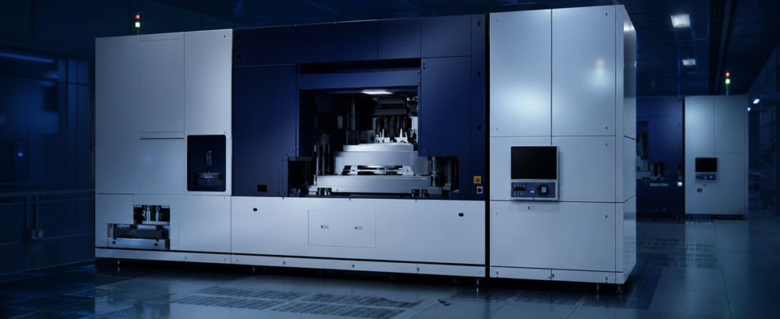
According to the available source information, Samsung Electronics has installed two High-NA EUV lithography systems but is holding back from putting them into mass production. The reported reason is financial: limiting depreciation expense and fixed overhead as the company’s foundry business works toward a return to profitability by Q4 2026.
That makes this more than an equipment-timing story. High-NA EUV is widely viewed as a major next step in advanced semiconductor manufacturing, but its adoption is also a capital-allocation decision. For foundries operating under margin pressure, the question is not only when a technology becomes available, but when its commercial use can be justified by demand, yields, and utilization.
For South Korea and the wider Asian semiconductor landscape, the reported pause highlights a central tension in advanced logic competition. Companies need to signal technological credibility at the leading edge, yet the cost of moving too early on expensive tools can weigh directly on profitability. Samsung’s reported caution may therefore reflect a broader reality of the AI-era semiconductor race: roadmap ambition has to be matched with financial endurance.
Watch the Short Brief
Watch this short visual briefing for the key strategic implications behind the story.
Key Developments
According to the report, Samsung is taking a cautious approach to deploying its two newly installed High-NA EUV systems into mass production. The available source information suggests the immediate driver is cost control rather than a retreat from advanced manufacturing.
The source summary links that decision to depreciation and fixed overhead management. In practical terms, this means Samsung appears to be trying to avoid bringing very expensive manufacturing assets fully into the cost base before the foundry business is in a stronger position to absorb them.
The same source information says the approach is tied to a profitability objective for the foundry business by Q4 2026. If accurate, that gives the decision a clear operational logic: preserve financial flexibility during a turnaround period rather than accelerate mass-production deployment for signaling value alone.
The development is also important because High-NA EUV sits near the frontier of lithography technology. In the broader industry, access to these systems matters because they are associated with future generations of advanced-node chipmaking. ASML is the established supplier of this class of EUV equipment, making adoption timing by major customers a closely watched indicator for the direction of the leading-edge manufacturing market.
What is not yet clear from the available information is whether Samsung’s move should be read as a short-term utilization delay, a slower production ramp, or a broader recalibration of timing for next-generation process deployment. That distinction matters for interpreting the competitive impact.
Strategic Analysis
The strategic significance of this report lies in the economics of timing. Installing cutting-edge semiconductor tools and using them at scale are not the same decision. Once advanced equipment is installed, the financial burden begins to build through depreciation and fixed plant costs, while the commercial benefits depend on process maturity, customer demand, and stable production yields.
That is why the reported delay matters. If Samsung is indeed prioritizing cost containment ahead of a foundry turnaround, the company may be signaling that near-term financial discipline currently outweighs the benefit of accelerating High-NA EUV into volume manufacturing. This does not necessarily imply reduced long-term ambition. It may instead suggest that Samsung is trying to sequence its investments more carefully.
One implication is that advanced-node competition is increasingly being shaped by capital efficiency as much as by technical capability. The leading edge of chip manufacturing has always been expensive, but the AI era has made the stakes even higher. Demand for advanced compute is rising, yet that does not eliminate the need for foundries to manage utilization, customer mix, and return on invested capital. Expensive tools that are underused can become a strategic burden rather than an advantage.
This is especially relevant in Asia, where semiconductor leadership is closely tied to industrial policy, export competitiveness, and supply-chain influence. South Korea’s technology position depends not only on Samsung’s ability to access frontier manufacturing tools, but also on its ability to deploy them in a financially sustainable way. A costly misstep at the leading edge can have implications beyond one business unit, affecting confidence in roadmap execution and in the resilience of the domestic semiconductor ecosystem.
There is also a broader competitive dimension. TSMC remains the central benchmark in advanced foundry manufacturing, and any company trying to narrow that gap must balance credibility with discipline. In that context, Samsung’s reported posture may reflect a practical view of the market: leading-edge participation is necessary, but absorbing the full cost of the next equipment generation before the economics are ready could deepen existing pressure rather than relieve it.
This makes High-NA EUV a useful lens for a larger industry shift. The next phase of foundry competition may not reward the fastest adopter in every case. It may reward the company that can combine selective technology deployment with better cost absorption, customer alignment, and operating leverage. If confirmed over time, Samsung’s reported restraint could be read as an attempt to compete more selectively rather than to match every milestone at maximum speed.
At the same time, the strategy carries risk. Advanced foundry customers often want confidence that a manufacturing partner can support future-node transitions on commercially relevant timelines. If a delay in mass-production use is interpreted as hesitation rather than discipline, Samsung could face tougher questions about roadmap competitiveness. The key issue is whether the company can preserve customer confidence while slowing the cost ramp.
That is why this report should be viewed as a potential tactical adjustment, not yet as proof of a deeper strategic shift. The available information supports the view that cost containment is the immediate rationale. It does not yet establish whether Samsung is merely delaying the production rollout of these tools or redefining the pace of its leading-edge manufacturing strategy.
Investor Takeaway
For investors and industry observers, the main signal is not simply that Samsung has High-NA EUV systems, but that it may be choosing not to monetize them through mass production immediately. That points to a disciplined reading of foundry economics during a turnaround phase.
The first issue to monitor is whether Samsung shows visible progress toward its reported Q4 2026 profitability objective in foundry. If that target remains central, the current High-NA posture may look less like hesitation and more like structured cost control.
Second, investors should watch for any change in language around equipment utilization and production timing. A future shift from cautious staging to active mass-production deployment would suggest that Samsung believes the commercial conditions have improved enough to absorb the additional cost base.
Third, customer confidence will matter as much as internal cost management. In advanced foundry markets, capex discipline only works if customers continue to view the manufacturing roadmap as credible. If Samsung can maintain that confidence while delaying the cost ramp, the strategy may strengthen the quality of its turnaround. If not, the pause could weigh on competitive positioning.
Fourth, the report reinforces a wider theme across the semiconductor sector: the next bottleneck is not always access to tools, but the economics of using them at scale. In the AI infrastructure cycle, investors often focus on technology milestones and capacity additions. This case is a reminder that utilization, depreciation, and timing remain critical variables in determining who converts expensive technology into sustainable returns.
In short, the reported decision may indicate that Samsung is trying to protect its foundry recovery before committing fully to the cost structure associated with next-generation lithography. For Asia’s semiconductor landscape, that is an important signal. The race for advanced manufacturing leadership is no longer just about who buys the most advanced equipment first. It is increasingly about who can deploy it without undermining financial stability.