Executive Summary
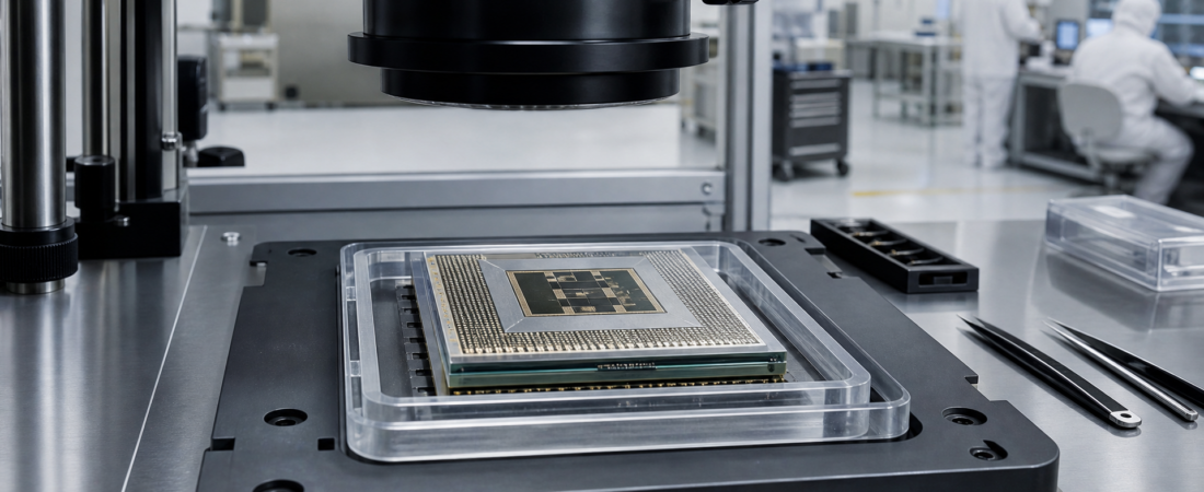
Intel has signed a memorandum of understanding with China-based Lens Technology to collaborate on advanced semiconductor packaging, according to the available source information. The reported focus is glass substrate-based packaging, specifically Through-Glass Via technology, with the stated aim of improving performance, interconnect density, and power efficiency for future AI and data center platforms.
The announcement matters because advanced packaging is becoming a more important competitive layer in the AI hardware stack. As chip scaling becomes harder and more expensive, performance gains increasingly depend on how processors, memory, and interconnects are integrated at the package level. In that context, a US semiconductor company and a Chinese manufacturing company exploring collaboration around glass substrate packaging is strategically notable even at the memorandum stage.
The key point for TechPowerAsia readers is not that a major supply-chain shift has already occurred. It has not. This remains an early-stage agreement rather than a disclosed commercial rollout. But the MoU may indicate that packaging-related capabilities are emerging as a distinct zone of cross-border interdependence, even as US-China tensions remain elevated across the broader semiconductor landscape.
Watch the Short Brief
Watch this short visual briefing for the key strategic implications behind the story.
Key Developments
– According to the source summary, Intel and Lens Technology have signed a memorandum of understanding covering advanced semiconductor packaging.
– The reported technical focus is glass substrate-based packaging and Through-Glass Via, or TGV, technology.
– The companies say the collaboration is intended to support higher performance, greater interconnect density, and improved power efficiency.
– The target applications identified in the available information are future AI and data center platforms.
– The two companies sit in different strategic jurisdictions: Intel in the United States and Lens Technology in China.
– Based on the disclosed information, the announcement is an MoU rather than a confirmed large-scale production agreement, and no investment size, binding commercial terms, or deployment timeline has been specified.
Strategic Analysis
Advanced packaging has become one of the semiconductor industry’s most important battlegrounds in the AI era. That is not just because leading-edge logic remains difficult to manufacture, but because the bottleneck has shifted upward into system integration. AI workloads increasingly depend on dense connections between compute, memory, and networking components, as well as better thermal and power characteristics across the full package. In practice, this means substrate technology, interconnect architecture, and packaging design now carry greater strategic weight than they did in earlier compute cycles.
That broader context makes Intel’s reported interest in glass substrate-based packaging understandable. Glass substrates are widely discussed in the industry as a possible route to improved dimensional stability, tighter interconnect capability, and better scaling potential for future high-performance packages. TGV technology is part of that conversation because it is designed to create vertical interconnect paths through glass, potentially supporting more complex package designs for AI and data center use cases.
The important qualification is that the current announcement does not establish commercial success. It signals intent to collaborate. For investors and industry readers, that distinction matters. The semiconductor sector is full of technology partnerships that begin with evaluation or development agreements and later change shape, slow down, or fail to progress into qualified production. The available source information supports a serious strategic signal, but not a confirmed packaging transition.
Even so, the cross-border dimension deserves attention. Much of the public US-China semiconductor debate has focused on front-end manufacturing, advanced nodes, lithography, and export controls. Packaging, materials, and precision process capabilities can receive less attention, yet they are increasingly central to AI hardware performance. This Intel-Lens Technology MoU may suggest that some areas of the semiconductor stack still operate through a more pragmatic logic of capability access and manufacturing specialization than through simple geopolitical alignment.
That does not mean packaging is insulated from politics. It means the dependency map may be more layered than the conventional decoupling narrative implies. A company may be heavily constrained in one part of the semiconductor value chain while still exploring cooperation in another. In this case, if the collaboration advances, it could highlight how advanced packaging sits at the intersection of performance engineering, materials science, and supply-chain geography.
The Asia angle is especially important. Across the semiconductor ecosystem, critical competencies are often distributed regionally rather than concentrated in a single national system. Precision manufacturing, specialty materials, substrate processing, and packaging integration are all areas where Asian companies have built meaningful leverage. From a TechPowerAsia perspective, this is the deeper signal: next-generation AI infrastructure depends not only on chip design and wafer fabrication, but also on the manufacturing ecosystems that can execute difficult packaging processes at scale.
Lens Technology’s presence in this announcement therefore matters beyond the company itself. According to the available source information, Intel is not merely discussing a generic research topic; it is naming a Chinese partner in an area tied to future AI and data center performance. That may indicate that packaging-related know-how and manufacturing capability remain globally relevant even in sectors under geopolitical scrutiny.
At the same time, readers should avoid overstating what this says about policy or supply-chain permanence. The announcement does not confirm regulatory clearance issues, long-term procurement commitments, or eventual product deployment. It also does not tell us whether Intel will qualify the technology for production programs, how broad the collaboration is, or whether it will remain limited to evaluation and development work. Those unknowns materially affect how much strategic weight to assign.
Still, there is a reason this development stands out. In an industry where the AI buildout is increasing pressure on every layer of hardware performance, advanced packaging is no longer a supporting detail. It is becoming part of the strategic core. If glass substrate approaches gain traction, the competitive advantage will not belong only to chip architects. It may also accrue to the companies and regions that can industrialize the underlying materials and packaging processes.
Investor Takeaway
The most useful way to interpret this announcement is as an early indicator, not a completed supply-chain shift. Intel and Lens Technology have signaled interest in collaborating on a packaging technology that aligns with the AI industry’s need for denser, more power-efficient system integration. That alone is enough to make the development worth tracking, particularly for readers focused on semiconductors, AI infrastructure, and cross-border industrial strategy.
Several monitoring points now matter.
First, investors should watch for signs that the MoU progresses beyond exploratory collaboration. The key question is whether Intel eventually discloses qualification, integration, or product-level adoption tied to glass substrate and TGV work. Without that progression, the announcement remains strategically interesting but commercially unproven.
Second, this development reinforces the need to follow advanced packaging as a separate strategic layer of the AI value chain. Front-end wafer leadership remains critical, but packaging is increasingly where system performance, power efficiency, and manufacturability converge. Companies with relevant capability in substrates, interconnect technologies, and precision materials processing may gain more attention as AI hardware roadmaps evolve.
Third, readers should monitor whether policymakers begin to pay greater attention to packaging-specific dependencies. If advanced packaging becomes more central to AI competitiveness, it could attract stronger regulatory and national security scrutiny over time. That would matter not only for Intel and Lens Technology, but for the broader map of US-Asia semiconductor relationships.
Finally, the announcement is a reminder that Asia’s role in the semiconductor industry extends well beyond foundries and assembly. The region’s manufacturing depth in materials, components, and process execution remains a strategic asset in the AI era. If glass substrate packaging develops into a meaningful commercial category, the balance of capability across the United States and Asia could become even more relevant to future data center and accelerator supply chains.
For now, caution is appropriate. The reported collaboration is meaningful as a signal, but not yet as proof of durable commercial change. The main implication is that advanced packaging may be emerging as one of the clearest areas where technical ambition, AI demand, and geopolitical complexity are starting to meet.