Executive Summary
A 7.1-magnitude earthquake in Japan’s southern Kyushu region on July 28 prompted Taiwan Semiconductor Manufacturing Co. to activate emergency evacuation procedures at its Kumamoto semiconductor facility, according to the available source information. TSMC later said all personnel were safe, structural inspections found no damage, and operations were gradually resuming.
On the immediate facts, the episode appears contained. No injuries were reported, no structural damage was disclosed, and there was no announced production, customer, or financial impact. Even so, the incident matters beyond a single day’s disruption because it highlights a core tension in Asia’s semiconductor build-out: efforts to diversify manufacturing geographically do not remove physical risk when new capacity is placed in earthquake-prone regions.
For TechPowerAsia readers, the significance is strategic rather than sensational. TSMC’s Kumamoto presence has been widely viewed as part of a broader effort to expand manufacturing outside Taiwan. This earthquake does not negate that logic, but it does show that geographic diversification in semiconductors must be judged through both geopolitical and environmental lenses. In the AI era, where steady chip output underpins everything from data-center build-outs to electronics supply chains, that distinction matters.
Watch the Short Brief
Watch this short visual briefing for the key strategic implications behind the story.
Key Developments
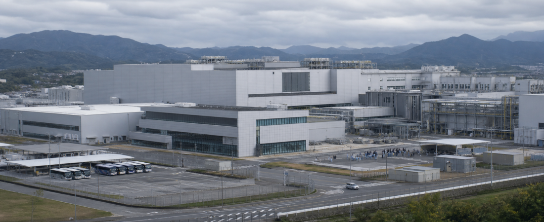
On July 28, a 7.1-magnitude earthquake struck southern Kyushu in Japan, leading TSMC to initiate emergency evacuation protocols at its Kumamoto facility, identified in the source information as JASM.
According to the report, the company later confirmed that all personnel were safe. It also said structural inspections showed no damage at the facility.
Based on those inspections, operations were allowed to gradually resume. The available source information does not specify the exact timing of the restart, any temporary production interruption, or whether wafer output was affected during the evacuation period.
No customer disruption, shipment adjustment, or financial effect was disclosed in the source information. That is important because semiconductor incidents often generate early speculation that outruns the facts. In this case, the reported picture remains narrow: evacuation, safety confirmation, no reported damage, and a staged return to normal operations.
The event also draws attention because Kumamoto is part of TSMC’s broader manufacturing footprint in Japan. While the source package lists Sony as a related company, the available information does not establish a specific operational impact on Sony or other companies tied to the regional electronics ecosystem. That broader linkage should therefore be treated as context, not as a confirmed consequence of this earthquake.
Strategic Analysis
The immediate operational outcome may be reassuring, but the broader strategic signal is harder to ignore. Semiconductor diversification is often framed as a response to geopolitical concentration risk, especially in relation to Taiwan. TSMC’s expansion in Japan fits into that wider industry discussion. What the Kumamoto earthquake highlights is that a strategy designed to reduce one category of risk can still leave companies exposed to another.
This is not a contradiction so much as a reminder that semiconductor resilience is multi-dimensional. A fab can be diversified geographically from a geopolitical standpoint and still remain vulnerable to local physical hazards such as earthquakes. Kyushu, like Taiwan, operates within a seismically active environment. The reported absence of damage at Kumamoto is therefore meaningful, but in a narrow way: it suggests the facility’s safety and engineering protocols held up in this instance. It does not remove the underlying exposure that comes with operating advanced industrial assets in earthquake-prone parts of Asia.
That matters because chipmaking is unusually sensitive to even short interruptions. Semiconductor fabrication depends on precise environmental control, tightly sequenced process flows, and equipment that can require careful recalibration after sudden shocks or stoppages. The available source information does not indicate that Kumamoto suffered those kinds of problems, and it would be wrong to infer them without evidence. Still, the event serves as a useful case study in how quickly a natural hazard can test an advanced manufacturing site, even when the eventual outcome is limited.
The implications extend beyond TSMC alone. Asia’s semiconductor map is being reshaped by parallel forces: geopolitical risk management, industrial policy, supply-chain regionalization, and the AI-driven need for dependable compute infrastructure. Japan has become an important location in that conversation because it offers industrial depth, engineering talent, and a policy environment supportive of semiconductor investment. The Kumamoto incident does not weaken those advantages. What it does suggest is that resilience planning for future fabs cannot stop at national diversification. Site selection, infrastructure hardening, emergency response, and restart capability all deserve greater attention.
There is also a communications dimension. In capital-intensive industries, incident response is judged not only by physical outcomes but also by how rapidly companies can establish operational clarity. According to the report, TSMC moved from evacuation to safety confirmation, inspection, and gradual resumption without public signs of severe damage. That sequence may help reassure customers and investors that the company’s procedures worked as intended. At the same time, markets will still want to know whether any later disclosures point to hidden frictions such as delayed output or altered delivery timing.
One reason this matters more in 2026 than it might have several years earlier is the strategic centrality of semiconductors to AI infrastructure. The AI build-out depends on a supply chain that is both technologically advanced and operationally stable. When a large foundry operator encounters a disruption scare, even a contained one, it becomes a lens through which policymakers, customers, and investors reassess concentration risk. The key question is not whether this specific earthquake caused a major supply shock; the available information suggests it did not. The more important question is whether the industry’s next wave of capacity additions is being designed with a sufficiently broad view of resilience.
Investor Takeaway
For now, the reported facts point to a contained operational event. Personnel were safe, no structural damage was reported, and operations were gradually resuming. That should limit the case for drawing dramatic conclusions from a single incident.
Even so, the earthquake is a useful monitoring trigger for investors and industry decision-makers. First, watch for any follow-up disclosure from TSMC on production continuity. A facility can avoid structural damage and still experience minor throughput disruption, but no such effect has been disclosed in the available source information.
Second, monitor whether the company or Japanese stakeholders say more about resilience measures at the site. Future commentary on backup systems, restart protocols, or additional hardening would be more informative than broad assurances alone.
Third, consider how this event fits into fab-siting logic across Asia. Semiconductor diversification remains strategically rational, especially where companies want to spread geopolitical exposure. But the Kumamoto episode underlines that diversification should not be interpreted as a complete solution. It changes the risk mix rather than eliminating risk altogether.
Fourth, keep the regional lens in focus. Asia remains the center of gravity for semiconductor manufacturing, and much of that capacity sits in areas exposed to natural hazards as well as geopolitical tension. For investors evaluating foundries, equipment suppliers, and downstream electronics manufacturers, the practical question is increasingly whether companies can demonstrate repeatable resilience under stress, not simply whether they have added more sites to the map.
In that sense, Kumamoto is best understood as a real-world systems test. Based on the information currently available, the site passed that test in the short term. The longer-term lesson is broader: in semiconductors, especially in the AI era, resilience depends not only on where capacity is built, but on how well that capacity can absorb shocks when they inevitably arrive.