Executive Summary
Samsung Electronics used FMS 2026 in the United States to present its next-stage memory roadmap for AI infrastructure, centered on two concept models — zHBM and zNAND-O — and what the company describes as the industry’s first V10 BV-NAND with more than 400 layers built using wafer bonding.
According to the available source information, the announcement was less about near-term commercialization than about signaling where Samsung believes AI infrastructure bottlenecks are moving. As AI systems scale, the challenge is no longer confined to accelerator compute. Memory bandwidth, density, packaging, and data movement are becoming increasingly important constraints at the system level.
For Asia technology and semiconductor watchers, Samsung’s roadmap matters because South Korea remains one of the most important centers in the global memory supply chain. When a company with Samsung’s manufacturing scale outlines a new memory direction, it offers an early read on where future capital spending, packaging requirements, and product competition may concentrate across the broader AI hardware stack.
Watch the Short Brief
Watch this short visual briefing for the key strategic implications behind the story.
Key Developments
At FMS 2026, Samsung showcased a set of AI memory initiatives that, taken together, point to a more vertically integrated approach to serving AI infrastructure.
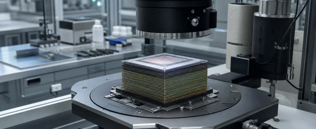
The most concrete disclosed element was V10 BV-NAND. Samsung presented it as the industry’s first NAND design exceeding 400 layers and said it was built using wafer bonding. Based on the available information, that distinction is important because it suggests Samsung is emphasizing bonding-based manufacturing techniques as a path to further NAND scaling, rather than relying only on more conventional layer expansion approaches.
Samsung also introduced zHBM and zNAND-O as concept models. The source material identifies zHBM as a vertical memory concept involving high-bandwidth memory and identifies zNAND-O as another next-generation memory concept, but it does not provide enough technical detail to support stronger claims about product specifications, performance metrics, or commercial readiness.
That matters for interpretation. V10 BV-NAND was presented with a specific manufacturing milestone, but zHBM and zNAND-O should be understood, based on the available source information, as architectural signals rather than confirmed shipping products.
The geographic relevance is also notable. Samsung is a South Korean technology champion operating in a sector that sits at the center of Asia’s semiconductor relevance to the AI era. The event itself took place in the United States, underlining how memory roadmaps are now being framed in a global AI infrastructure context rather than only within traditional storage markets.
What the announcement did not establish is just as important. The available source information does not confirm customer commitments, volume production schedules, pricing, sampling status, or commercial deployment timelines for the new concepts. It also does not provide sufficient support for detailed performance claims beyond Samsung’s high-level positioning of the technologies.
Strategic Analysis
Samsung’s FMS 2026 presentation points to a broader shift in semiconductor strategy: AI memory is increasingly becoming an architectural battleground, not just a component category.
For much of the AI buildout cycle, investor attention has centered on accelerator logic, foundry capacity, and packaging bottlenecks. Those remain critical. But the more AI systems scale, the more memory design becomes a determining factor in overall system efficiency. High-performance accelerators are only as effective as the memory systems that can feed them, and the value of memory vendors may increasingly depend on how tightly their products can be integrated into AI compute architectures.
That is one of the most important implications of Samsung’s zHBM concept. Even without overstating technical specifics that are not confirmed in the source packet, the reported direction suggests a deeper integration of memory with AI accelerators. If that direction advances into production over time, it could shift competitive emphasis away from standalone memory specifications and toward co-design across memory, packaging, and compute.
This would have direct implications for the Asian semiconductor ecosystem. South Korea’s leading position in memory gives it structural importance in AI hardware, but the next phase may depend not only on wafer fabrication scale. It may also depend on success in advanced integration techniques, packaging collaboration, and system-level qualification with accelerator partners. In other words, memory leadership in the AI era may increasingly be judged by how effectively suppliers participate in platform architecture, not only by density or cost per bit.
V10 BV-NAND carries a different but related signal. NAND has long relied on vertical layer scaling, but moving beyond 400 layers through wafer bonding may indicate that manufacturing complexity is becoming a more strategic differentiator. If accurate, this could point to a future in which bonding capability, yield control, and process integration become more central to competitive positioning in advanced NAND.
That matters because wafer bonding is not just a process detail. It can influence equipment demand, defect management, throughput economics, and the broader supplier ecosystem. For Asia, where semiconductor capital expenditure and equipment localization are major strategic questions, any shift toward more bonding-intensive memory production could ripple across tool vendors, materials suppliers, and backend process specialists.
The announcement also reinforces a basic but increasingly important market reality: only a small number of companies can credibly shape the top end of AI memory supply. Samsung’s significance therefore extends beyond its own product roadmap. Its public technology signaling can affect expectations for rivals, customers, and equipment makers across the global supply chain.
At the same time, caution is essential. Company presentations at industry events often serve multiple purposes: technology positioning, ecosystem signaling, recruitment of partners, and competitive messaging. That does not diminish their importance, but it does mean roadmap announcements should not be treated as equivalent to broad commercial adoption. The key distinction here is between demonstrated direction and validated market deployment.
For TechPowerAsia readers, the most useful interpretation is not that Samsung has already resolved AI memory bottlenecks, but that it is publicly aligning its roadmap around the problems most likely to define the next stage of AI infrastructure: bandwidth pressure, integration density, and manufacturing pathways that can support both.
Investor Takeaway
The immediate relevance of Samsung’s FMS 2026 announcement lies more in strategic direction than in short-term revenue visibility.
First, investors should view the presentation as evidence that memory architecture is moving closer to the center of AI infrastructure competition. That raises the importance of tracking not only HBM supply growth, but also the degree to which memory suppliers can extend into packaging-intensive and accelerator-adjacent designs.
Second, V10 BV-NAND is worth watching as a signal on manufacturing method. If wafer bonding becomes a more meaningful route for ultra-high-layer NAND, the effects may extend beyond Samsung to equipment makers, materials providers, and process specialists exposed to advanced memory fabrication. The key question is whether this remains a technology showcase or becomes a repeatable commercial manufacturing path.
Third, the Asia angle is significant. South Korea is already central to the memory supply chain, and Samsung’s roadmap choices may influence how the region’s semiconductor capital and industrial capabilities are deployed in the AI era. If future AI infrastructure places greater value on tightly integrated memory subsystems, Asia’s role in memory production could become even more strategically important — provided suppliers can translate roadmap ambition into manufacturable products.
What should readers monitor next? The most important indicators are whether Samsung provides clearer commercialization signals for zHBM and zNAND-O, whether outside customers or ecosystem partners validate these architectures, and whether competing memory manufacturers reveal similar vertical integration strategies. Broader adoption of comparable approaches would suggest an industry shift; limited follow-through would suggest that, for now, the announcement remains primarily a forward-looking technology statement.
The bottom line is that Samsung’s FMS 2026 unveiling should be read as an early indicator of where AI memory competition may be heading. It does not by itself confirm near-term market transformation. But it does sharpen the strategic focus on a critical issue for the AI era: future infrastructure performance may depend as much on how memory is built and integrated as on how fast the accelerator itself becomes.