Executive Summary
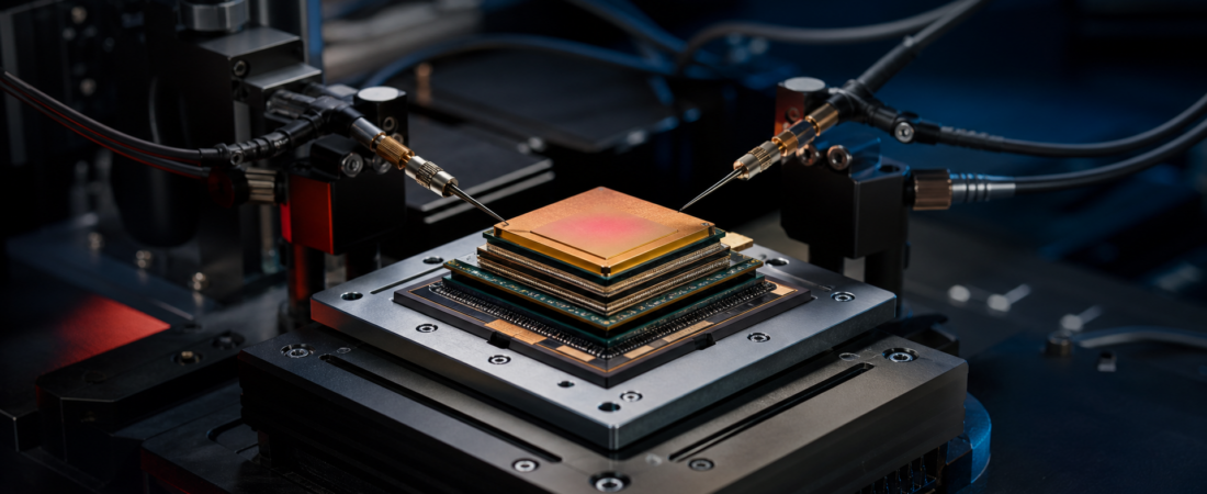
According to the available source information, chip packaging experts are increasingly framing heat dissipation as the main bottleneck for 3D-stacked AI chips. The report points to co-packaged optics, or CPO, and system-technology co-optimization, or STCO, as emerging approaches that may help manage this constraint.
That framing matters because it shifts attention away from a familiar semiconductor question, how many more transistors can be packed onto a chip, toward a harder system question: how much performance can be sustained once compute, memory, and interconnect are pushed into denser physical configurations. In advanced AI hardware, packaging is no longer just a downstream manufacturing step. It is becoming part of the performance equation.
For Asia’s technology ecosystem, this is strategically relevant even without company-specific announcements. The region sits at the center of semiconductor manufacturing, assembly, materials, and optical supply chains. If thermal limits become a defining bottleneck for next-generation AI systems, the competitive focus may increasingly extend beyond leading-edge fabrication and into packaging architecture, interconnect design, and system-level engineering.
Watch the Short Brief
Watch this short visual briefing for the key strategic implications behind the story.
Key Developments
According to the report, industry specialists in chip packaging see heat as the primary constraint on further gains from 3D-stacked AI chips. The core issue is not that stacking has lost its value, but that adding more compute density can make it harder to remove heat efficiently.
The available source information highlights two solution paths in particular.
First, co-packaged optics is presented as a potentially important technology. In broad industry terms, CPO refers to bringing optical interconnects closer to compute and networking silicon. The strategic appeal is that data movement is increasingly a major system challenge in AI infrastructure, and optical approaches may help reduce some of the power and thermal burden associated with electrical interconnects.
Second, system-technology co-optimization is identified as another possible response. STCO is a design approach that looks at chip, package, interconnect, and system considerations together rather than optimizing each layer in isolation. The implication is that thermal management may no longer be solvable through chip design alone.
The report, based on the available summary, appears to be an industry-perspective piece rather than coverage of a specific product launch, corporate investment, or government policy action. No individual companies, production schedules, performance targets, or commercialization timelines are provided in the source information available here.
That distinction is important. The report signals where expert concern is focusing, but it does not by itself confirm which firms will lead, how quickly these approaches will scale, or which solution set will prove most commercially effective.
Strategic Analysis
The deeper significance of this report is that it reflects a broader change in where semiconductor performance gains may increasingly be won or lost.
For much of the industry’s history, the central performance story was transistor scaling. That logic still matters, but in AI hardware the bottlenecks are spreading outward from the logic die into packaging, memory proximity, interconnect bandwidth, and power delivery. The source’s emphasis on heat suggests that advanced AI performance is becoming a multi-variable system problem rather than a purely lithography-driven one.
3D stacking illustrates the opportunity and the trade-off. Stacking can improve performance, bandwidth, and integration by placing critical functions closer together. But denser physical integration can also trap heat, complicate thermal paths, and raise design constraints at the package and system level. In that environment, the industry may not be able to assume that more density automatically translates into practical, scalable performance.
That is where the report’s focus on CPO and STCO becomes strategically meaningful.
CPO matters because AI systems are increasingly defined not only by raw compute, but also by how efficiently data moves between processors, memory, and network elements. If optical interconnects can reduce part of the electrical and thermal burden around high-speed data movement, they could become an important complement to dense packaging. The key point is not that CPO is already the dominant answer, but that the thermal discussion is expanding beyond the chip package itself into the architecture of the full AI system.
STCO matters because it reflects a change in design philosophy. When thermal, power, packaging, and system constraints interact closely, optimizing a single component in isolation can produce diminishing returns. A system-level approach may therefore become more important in deciding how AI chips are partitioned, packaged, connected, and cooled. If that pattern strengthens, semiconductor competition could increasingly depend on cross-domain integration rather than excellence in only one layer of the stack.
For Asia, this raises a meaningful strategic question. Much of the global semiconductor ecosystem for fabrication, packaging, memory, substrates, components, and electronics manufacturing is concentrated in Asia, especially across East Asia. If the center of engineering difficulty moves further toward thermal management, advanced packaging, and system integration, that could increase the strategic importance of the region’s broader semiconductor supply chain, not just its wafer-fabrication base.
That does not mean competitive advantage automatically shifts to any one country or company. The available source information does not support that conclusion. But it does suggest that investors and industry planners may need to pay closer attention to where packaging know-how, optical integration capability, and thermal engineering depth are developing.
There is also a wider AI infrastructure implication. If heat becomes the practical ceiling for denser accelerator deployment, then scaling AI compute is not simply a matter of procuring more advanced chips. It may increasingly depend on how efficiently those chips can be packaged, interconnected, and operated within broader power and cooling limits. In that sense, thermal bottlenecks could influence not only semiconductor roadmaps, but also the economics of AI system deployment.
Still, caution is warranted. The report identifies a problem and points to possible solution paths, but it does not establish that CPO or STCO will resolve the issue at commercial scale in the near term. Thermal management in AI systems can also involve other approaches, including cooling technologies, architectural trade-offs, and different packaging choices. The strategic takeaway is therefore not that a single answer has emerged, but that the industry’s constraint set is changing.
Investor Takeaway
The most useful way to read this development is as an early signal about where semiconductor attention and capital may increasingly flow if thermal constraints continue to intensify in AI hardware.
One area to watch is advanced packaging. If heat remains the limiting factor in 3D-stacked AI designs, packaging capability could become even more central to performance differentiation. Investors should monitor whether packaging discussions move from manufacturing capacity alone toward thermal architecture, material choices, and system integration.
A second area is optical interconnect. The report’s focus on CPO suggests that data movement and thermal efficiency are becoming more tightly linked. The key question is whether optical approaches begin moving from long-term promise toward clearer product adoption in AI systems and networking infrastructure.
A third area is design methodology. STCO may sound abstract, but strategically it points to a more integrated model of semiconductor development. Investors should monitor whether more companies begin talking about chip-package-system co-design, and whether that language appears in product roadmaps, packaging partnerships, or capital allocation priorities.
For Asia-focused readers, the practical implication is to watch the full semiconductor stack rather than only leading-edge logic. If the reported concern over heat proves durable, the most relevant signals may come from packaging ecosystems, memory-adjacent technologies, materials, photonics, and system integration capabilities across the region.
At this stage, the report is best understood as a directional indicator, not a near-term catalyst tied to a named company or specific timetable. But it does sharpen a critical point for the AI era: as compute density rises, the next bottleneck may be less about how much silicon can be built and more about how much performance can be sustained once heat becomes the binding constraint.