Executive Summary
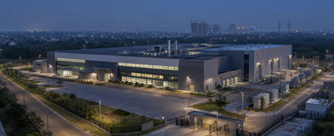
Applied Materials has announced a long-term semiconductor investment plan in India that could carry significance beyond its headline size. According to the available source information, the company unveiled an “India Vision 2035” initiative at SEMICON India 2026, committing $5 billion over the next decade to build a 140-acre advanced semiconductor research park and expand its local supply-chain capacity tenfold.
For India, the strategic importance is not just the dollar amount. The reported plan sits in the upstream part of the semiconductor value chain, where equipment, process know-how, and specialized supplier networks matter as much as fabrication capacity itself. That makes this announcement different from more downstream manufacturing activity, because semiconductor equipment capability can shape whether a broader domestic chip ecosystem becomes more technically embedded over time.
For Asia technology investors and industry strategists, the announcement may indicate that India is attracting interest not only as an electronics manufacturing base, but also as a location for deeper semiconductor infrastructure. The key question now is execution: whether the reported commitment translates into physical assets, supplier expansion, and a durable local capability base over the next decade.
Watch the Short Brief
Watch this short visual briefing for the key strategic implications behind the story.
Key Developments
According to the source summary, Applied Materials announced a $5 billion investment plan for India to be deployed over 10 years under its “India Vision 2035” program.
The announcement was made at SEMICON India 2026, a relevant venue given India’s effort to raise its profile in the semiconductor industry.
The reported plan includes two core elements:
– construction of a 140-acre advanced semiconductor research park in India
– a tenfold expansion of Applied Materials’ local supply-chain capacity over the coming decade
The available information does not provide a detailed allocation of the $5 billion across facilities, supplier development, equipment, workforce, or other categories. It also does not specify site location, intermediate milestones, policy support, or the measurement baseline for the reported tenfold supply-chain expansion.
Those omissions matter. Large semiconductor-related announcements often span multiple phases, and the difference between a strategic framework and an operational buildout can be substantial. At this stage, the clearest confirmed point is that Applied Materials has outlined a decade-long India commitment tied to research infrastructure and supply-chain scaling.
Strategic Analysis
The most important aspect of this announcement is where Applied Materials sits in the semiconductor stack. Semiconductor equipment companies occupy a highly specialized layer of the industry, supplying the tools and process technologies used to manufacture chips. That layer is upstream, technically demanding, and difficult to localize quickly.
This is why the reported India plan stands out. A research park and supply-chain expansion from an equipment company may have different implications from a pure assembly, testing, or packaging announcement. It suggests a possible move toward embedding more technical and supplier capability inside India’s semiconductor ecosystem rather than limiting local activity to downstream operations.
That distinction matters for Asia’s broader semiconductor geography. The region’s chip industry has historically clustered in established manufacturing and R&D hubs, with different countries specializing in design, foundry production, packaging, materials, or equipment-related capabilities. If a company such as Applied Materials scales meaningful local infrastructure in India, it could gradually widen India’s role in the regional semiconductor landscape.
This should still be framed carefully. The available source information does not indicate that India is about to become a major equipment manufacturing hub, nor does it confirm the precise technical scope of the planned research park. But one strategic implication is clear: an upstream investment of this kind may help deepen local industrial capability more effectively than isolated downstream projects alone.
The supply-chain angle is equally important. Semiconductor equipment production depends on a network of precision components, subassemblies, specialty materials, engineering services, and rigorous quality systems. A reported goal of expanding local supply-chain capacity tenfold suggests that Applied Materials is not just discussing a standalone site investment. It may also be trying to build or expand a broader domestic support base around its India operations.
If that happens, the effects could extend beyond one company. Supplier localization often creates second-order opportunities for adjacent firms, including precision manufacturing companies, component makers, cleanroom infrastructure providers, and specialized industrial service groups. The source information does not confirm any follow-on commitments from other companies, so that broader ecosystem effect remains a scenario rather than an established trend. But it is a key dynamic to watch.
There is also a capital allocation signal here. In semiconductors, long-duration commitments tend to matter because the sector is capital intensive, technically interdependent, and slow to scale. A decade-long plan can indicate that a company sees enough strategic value in the location to justify a phased buildout rather than a short-term commercial expansion. For India, that matters because it points to a potential shift from policy ambition toward harder industrial infrastructure.
From an Asia supply-chain perspective, this announcement also fits a wider pattern of geographic diversification. Across semiconductors and related technologies, companies have increasingly evaluated where to place manufacturing, engineering, and supplier networks in response to resilience concerns, geopolitical friction, and concentration risk. The available source information does not state that Applied Materials’ India plan is driven by these factors, so that should not be presented as confirmed company rationale. Even so, the move can reasonably be viewed within the broader regional context of supply-chain diversification.
The research park component deserves special attention. In semiconductor strategy, R&D-linked infrastructure can carry more long-term value than a headline factory announcement if it helps create localized engineering capability, process development, and stronger links between industry and domestic technical talent. The source summary identifies the project as an advanced semiconductor research park, but does not describe its intended research scope or operating model. Investors should therefore avoid overreading the term. Still, even at a high level, the inclusion of research infrastructure suggests that the plan is not framed solely around commercial sales expansion.
For India, this development may also strengthen the argument that success in semiconductors requires more than incentives for end-stage manufacturing. Upstream capability depends on ecosystem density: suppliers, technical skills, equipment servicing, process knowledge, and long planning cycles. The reported Applied Materials commitment does not solve those constraints by itself, but it may represent movement in a more structurally important direction.
Investor Takeaway
Investors should view this announcement as a long-horizon strategic signal rather than a near-term operating catalyst.
The reported $5 billion commitment is material, but the investment case will depend far more on execution than on the headline figure alone. Over the next several years, the main issue is whether Applied Materials converts its India Vision 2035 framework into visible infrastructure, supplier development, and measurable local capacity expansion.
Several markers will be worth tracking:
– project execution: confirmation of site development, construction progress, and any phased commissioning of the reported research park
– supply-chain buildout: evidence of new supplier onboarding, localization of components or services, and clearer definitions of how the tenfold capacity target will be measured
– policy framework: any disclosed details on state or national government support, land arrangements, infrastructure access, or regulatory facilitation
– ecosystem response: whether other semiconductor equipment, materials, or precision manufacturing players announce related India investments
– strategic positioning: whether India begins to attract more upstream semiconductor activity alongside downstream manufacturing initiatives
There are also important risks. Ten-year industrial commitments can be delayed, resized, or re-sequenced. Semiconductor demand cycles, cross-border technology policy, infrastructure readiness, and talent availability can all affect outcomes. In addition, the available source information does not provide enough detail to judge the pace or exact scope of the proposed buildout.
That means investors should be careful not to extrapolate too far from the initial announcement. One company’s plan, even from an important industry participant, does not by itself redefine India’s position in the semiconductor value chain.
Even so, the announcement deserves attention. If executed broadly as described, it could mark a meaningful step in India’s push to move deeper into the semiconductor stack and could reinforce Asia’s ongoing reconfiguration of technology supply chains around resilience, capability, and long-term capital commitment.