Executive Summary
Samsung Electronics and ASML have expanded their strategic partnership to advance High Numerical Aperture extreme ultraviolet lithography and support a transition to 12-inch photomask technology, according to the available source information. The reported target is high-volume DRAM production by 2028.
That makes this less a near-term product story than a roadmap signal about where memory manufacturing is heading. For Asia’s semiconductor ecosystem, the significance lies in the combination of process technology, equipment access, and supply-chain coordination required to move advanced DRAM into its next scaling phase.
The reported partnership also highlights a broader industry reality: in advanced semiconductors, competitive advantage increasingly depends not only on chip design and end demand, but on who can secure and industrialize the most critical manufacturing tools. In that sense, a deeper Samsung-ASML relationship may indicate how Korea’s memory champion is preparing for the next stage of process competition.
Watch the Short Brief
Watch this short visual briefing for the key strategic implications behind the story.
Key Developments
According to the report, Samsung Electronics and ASML have expanded their existing strategic partnership with a focus on two core areas.
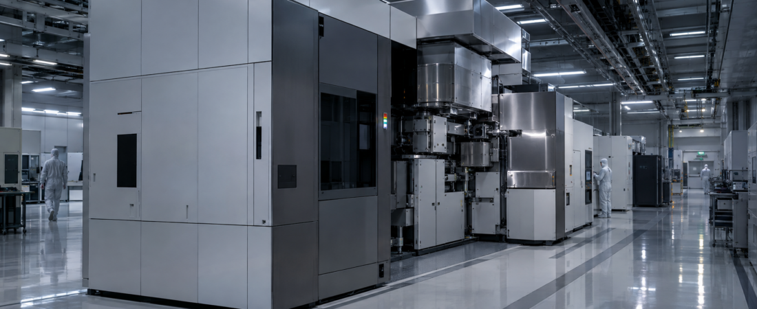
First, the collaboration is centered on next-generation High-NA EUV lithography. High-NA is widely viewed as the next major advance beyond current EUV systems, offering finer patterning capability for increasingly complex semiconductor processes.
Second, the partnership includes a transition toward 12-inch photomask technology. The source information frames this as a move beyond the current 6-inch standard used in the industry.
The stated objective is high-volume DRAM production by 2028. Based on the available information, that is the clearest timeline marker attached to the partnership.
The companies involved are Samsung Electronics of South Korea and ASML of the Netherlands. That cross-border alignment matters strategically: Samsung remains one of Asia’s most important memory manufacturers, while ASML occupies a central position in the global lithography equipment chain.
Beyond those points, the available source information does not provide detail on investment size, contract terms, capacity targets, specific tool models, or intermediate milestones. As a result, the development is best understood at this stage as a roadmap-level partnership expansion rather than a fully quantified manufacturing plan.
Strategic Analysis
The partnership matters because lithography has become one of the most important constraints on semiconductor progress. As memory manufacturers push to increase density and performance, the complexity of transferring chip designs onto silicon rises sharply. That makes access to the next generation of patterning tools a strategic issue, not simply an engineering upgrade.
For Samsung, the reported High-NA EUV focus may indicate an effort to secure an early position in the next phase of DRAM scaling. If the 2028 target holds, the company would be aligning tool development, mask technology, and process integration over a multi-year period rather than waiting for a later, more reactive transition. In a capital-intensive industry, timing matters: moving too early can raise cost and execution risk, while moving too late can weaken long-term competitiveness.
The photomask component is also notable. Lithography discussions often focus on scanners, but mask infrastructure is a critical part of the production ecosystem. A transition from 6-inch to 12-inch photomasks could imply broader changes across tooling, materials, inspection, and process control. In other words, the shift is not just about one machine vendor and one chipmaker. It may require a wider industrial adjustment across the semiconductor supply chain.
That has direct relevance for Asia. South Korea is a core node in global memory production, and changes in Samsung’s manufacturing roadmap can influence equipment demand, supplier planning, and competitive expectations across the region. Even when the headline names are Samsung and ASML, the downstream effects can extend to Asian materials providers, mask-related suppliers, and process ecosystem partners.
This development also fits a larger trend in which advanced memory becomes more important to AI infrastructure. The source information does not explicitly tie the partnership to AI workloads, and that distinction matters. Still, from a strategic perspective, any credible path to more advanced, high-volume DRAM later this decade is likely to be read against rising compute and memory requirements across AI systems. Memory performance, density, and manufacturability are increasingly part of the same conversation as accelerators and data-center buildouts.
Another implication is the persistence of supplier concentration. ASML’s role in advanced lithography means that any leading-edge roadmap involving EUV remains connected to a narrow part of the equipment chain. That creates structural dependence for chipmakers pursuing the most advanced process paths. A deeper Samsung-ASML partnership may help alignment and planning, but it does not remove the concentration risk embedded in the current ecosystem.
From a geopolitical and industrial-policy perspective, the story is also relevant because it links a major Asian manufacturer with one of Europe’s most strategically important semiconductor equipment companies. Advanced chip production increasingly depends on cross-border coordination among a small group of companies operating under growing technology, export-control, and supply-chain scrutiny. Even when a partnership is commercial in nature, it sits inside a broader environment where semiconductor capability is treated as strategic infrastructure.
The competitive implications should be framed carefully. The available source information does not provide timelines or comparable plans from Samsung’s rivals. But it is still reasonable to interpret this move as part of a wider contest over who can maintain cost-effective scaling in memory. If High-NA EUV and larger photomasks become important for next-generation DRAM, then industrializing those technologies could shape relative positioning across the memory sector over time.
What remains uncertain is execution. High-NA EUV is technically ambitious, and any transition of this kind typically carries challenges around integration, throughput, defect management, and ramp timing. The 2028 high-volume production target gives investors a useful reference point, but the path between partnership expansion and volume manufacturing is likely to be demanding.
Investor Takeaway
The reported Samsung-ASML partnership should be viewed as a long-duration semiconductor manufacturing signal rather than an immediate earnings catalyst. Its importance lies in what it suggests about the future of memory process technology, capital intensity, and ecosystem coordination.
For investors tracking Asia technology, several issues now matter.
The first is milestone visibility. Investors should monitor whether Samsung and ASML disclose concrete progress on High-NA EUV integration, pilot readiness, or mask-transition infrastructure over the next several years. Roadmap announcements carry more weight when they are followed by operational markers.
The second is capital allocation. Advanced lithography transitions are expensive, and the scale of future equipment purchases, facility upgrades, or related supply-chain investment could help clarify how serious and how near-term this effort is. Any later disclosures in that direction would be important confirmation signals.
The third is ecosystem follow-through. If the 12-inch photomask transition gains traction, related suppliers in masks, materials, metrology, and inspection may begin to reflect that shift in their own plans. That could offer an earlier read on whether the reported partnership is isolated or part of a broader industry transition.
The fourth is execution risk. Even strategically sound technology moves can face delays, higher costs, or slower-than-expected manufacturing ramps. Investors should be careful not to assume that partnership expansion automatically translates into commercial success on schedule.
Finally, the development reinforces a broader theme central to TechPowerAsia’s coverage: the future of AI-era semiconductor competition will be shaped as much by manufacturing infrastructure and tool access as by end-market demand. According to the available source information, Samsung and ASML are positioning around that reality now, with a reported goal of high-volume DRAM production by 2028. Whether that target is met will determine how much this partnership ultimately changes the balance of advantage in advanced memory.