Executive Summary
According to the available source information, TSMC, Intel, and Samsung Electronics are aligning with Applied Materials through its EPIC Center to co-optimize 3D packaging and advanced-node architectures for AI chips. If sustained, that would mark an important shift in how leading semiconductor companies approach the next stage of AI hardware development.
The reported significance is not simply that three major chipmakers are working with a key equipment supplier. It is that the collaboration is framed around earlier technology integration, suggesting that manufacturing tools, packaging approaches, and chip architecture choices may need to be considered together much earlier in the development cycle.
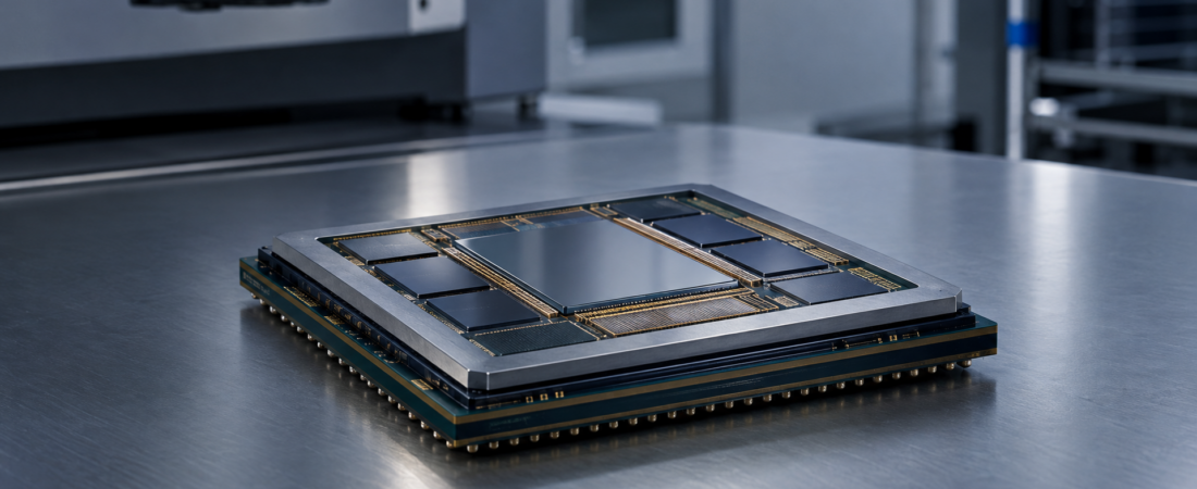
For AI silicon, that matters because performance is no longer determined by transistor scaling alone. Advanced packaging, interconnect density, power delivery, and thermal constraints are becoming increasingly important in how next-generation accelerators are designed and produced. In that context, the reported alignment around early co-optimization may indicate that competitive advantage is shifting toward ecosystem-level execution rather than node leadership alone.
For Asia, the development is especially relevant. TSMC and Samsung are central to the region’s advanced semiconductor position, while Taiwan, South Korea, and the United States remain deeply interconnected across design, manufacturing equipment, and production capacity. A move toward earlier co-development across these hubs could have implications for supply-chain structure, capital allocation, and the geography of AI chipmaking.
Watch the Short Brief
Watch this short visual briefing for the key strategic implications behind the story.
Key Developments
According to the source summary, TSMC, Intel, and Samsung Electronics are engaging with Applied Materials through the EPIC Center on the co-optimization of 3D packaging and advanced-node architectures for AI chips.
The reported emphasis on early technology integration is the central point. Rather than treating manufacturing equipment and packaging as downstream execution issues, the companies appear to be addressing them earlier in the process. That suggests the technical challenges associated with AI chips may be difficult to solve through conventional handoffs between chip designers, foundries, and equipment suppliers.
The geographic footprint is also notable. The companies involved span three major semiconductor centers: Taiwan, South Korea, and the United States. That gives the development broader relevance than a single-company R&D effort, particularly for observers tracking where advanced AI manufacturing capability is being coordinated and reinforced.
At the same time, the available information remains limited. The report summary does not provide financial commitments, production timelines, product names, or formal details on the structure of the collaboration. It also does not specify whether the work is pre-competitive research, product-oriented development, or a broader long-term integration model. Those distinctions will matter in assessing how strategically meaningful the reported alignment becomes.
Strategic Analysis
The most important takeaway is that the industry’s next AI manufacturing bottlenecks may be less about shrinking transistors in isolation and more about integrating multiple technology layers at once.
That is where 3D packaging becomes strategically important. AI accelerators increasingly depend on the efficient connection of compute, memory, and I/O within strict power and thermal limits. Advanced packaging has already become a major area of competition in AI hardware, and the reported focus on co-optimization suggests that packaging may no longer be treated as a late-stage packaging problem alone. Instead, it may need to be designed in parallel with process technology and system architecture.
If that interpretation is accurate, one implication is that equipment makers could become more deeply embedded in defining what next-generation AI chips are practical to manufacture. Historically, semiconductor equipment suppliers have always been essential, but the traditional model often positioned them as executing against roadmaps largely set by chipmakers and foundries. Earlier integration could shift that balance somewhat, making manufacturing tool capabilities a more direct factor in product architecture choices.
That does not mean proprietary competition disappears. TSMC, Intel, and Samsung remain direct rivals in advanced manufacturing and packaging. But the reported alignment may suggest that at least some frontier AI chip challenges are difficult enough to justify earlier shared work with major equipment partners. In practical terms, this could signal that solving AI-era semiconductor constraints increasingly depends on tighter coordination across process, packaging, and equipment ecosystems.
For Asia, that possibility carries strategic weight. Taiwan and South Korea are already central to global semiconductor capacity and know-how, especially in advanced manufacturing. If earlier co-development with equipment suppliers becomes more common, Asia’s role in the AI hardware stack could deepen further—not just as a production base, but as a core site of technical integration. That would reinforce the region’s relevance across semiconductors, supply chains, and AI infrastructure.
There is also a geopolitical angle, even if the reported information does not point to any specific government role. Taiwan, South Korea, and the United States are simultaneously partners and competitors in semiconductor strategy. Cross-border technical alignment can support leadership at the frontier, but it also exists alongside national efforts to localize capacity, secure supply chains, and reduce strategic dependence. The tension between ecosystem collaboration and industrial sovereignty is therefore likely to remain an important backdrop.
Applied Materials’ position is worth watching in that context. If equipment suppliers are pulled earlier into AI chip development, the value of their role may become more strategic, not just operational. That would not automatically translate into commercial gains, but it could alter how investors and industry planners assess leverage within the semiconductor value chain. The companies that help define manufacturability at the frontier may become more important in setting the pace of AI infrastructure deployment.
Still, caution is necessary. The current report supports a meaningful signal, not a definitive industry realignment. It is not yet clear how deep the collaboration runs, whether it will produce differentiated manufacturing outcomes, or how much of the work is exploratory rather than directly tied to future production programs. The strategic interpretation is compelling, but the evidence currently available remains limited to the reported alignment and its stated technical focus.
Investor Takeaway
For investors and strategic observers, the reported development is best understood as an early indicator of where AI semiconductor competition may be heading.
First, monitor whether advanced packaging continues to rise as a core measure of leadership alongside process-node capability. If future disclosures from TSMC, Intel, and Samsung place greater emphasis on integrated packaging and architecture development, that would support the view that AI chip competitiveness is being redefined more broadly.
Second, watch the equipment layer more closely. If companies such as Applied Materials are increasingly referenced in early-stage development efforts rather than only in capex cycles, that could suggest a more embedded role in shaping next-generation AI manufacturing paths.
Third, track capital allocation. The available report does not provide spending figures, but any later expansion in packaging R&D, pilot-line investment, or advanced integration capacity would be an important confirmation signal. Early technical alignment matters most when it is followed by visible resource commitment.
Fourth, pay attention to the durability of cross-border coordination. The involvement of Taiwan, South Korea, and the United States underscores how interconnected advanced semiconductor leadership remains. The key question is whether that coordination expands despite policy frictions, or whether national industrial priorities begin to limit the depth of collaboration.
Finally, investors should resist reading too much into the report too quickly. The development may prove significant, but its practical impact will depend on whether early co-optimization leads to better yields, improved performance-per-watt, faster deployment cycles, or stronger customer adoption in AI hardware markets. Those outcomes are not yet established by the available information.
What is clear is that the next bottleneck in AI chipmaking may be pushing the industry to coordinate earlier and more closely across the manufacturing stack. For Asia’s semiconductor leaders, that is a signal worth taking seriously.