Latest posts
-
ASML Extends Lithography Lead as Asian Chipmakers Prepare for High NA
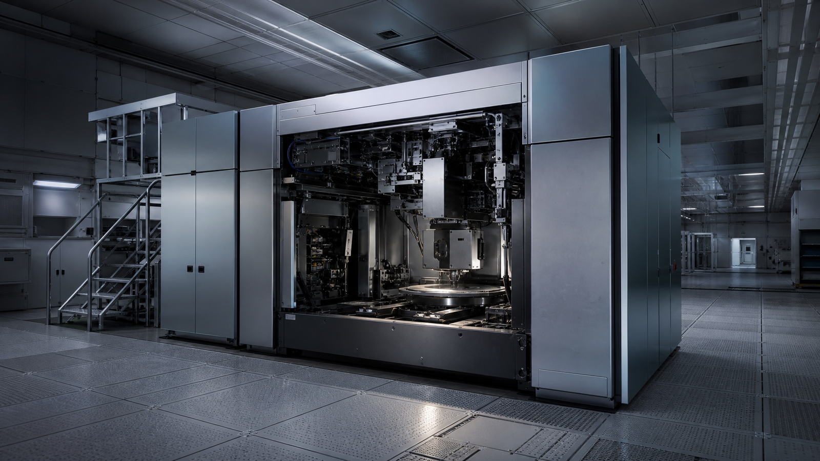
ASML’s EUV tools are reportedly sold out through 2027, while TSMC, Samsung, and SK Hynix target High NA production from 2028. The shift could make tool access and delivery timing a major constraint on Asia’s advanced chip roadmaps.
-
TSMC’s Reported 2027 Capacity Push Puts 2nm, 3nm, and CoWoS at the Center of AI Supply
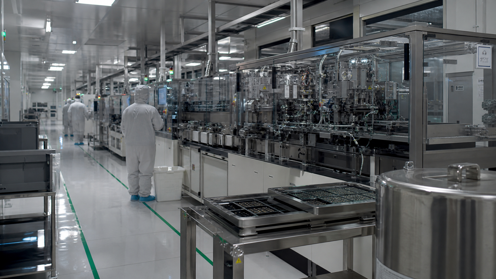
TSMC’s reported expansion is strategically important because it pairs leading-edge wafer growth with a plan to double CoWoS packaging. The result is a clearer view of where AI hardware supply may still be constrained.
-
Singapore and Malaysia Split the Advanced Packaging Value Chain
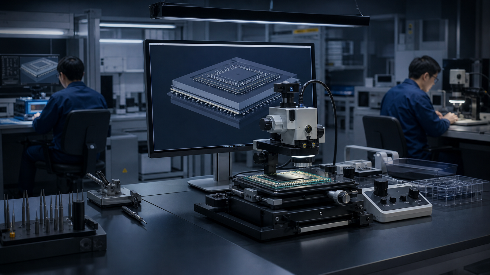
Singapore and Malaysia appear to be taking different roles in advanced packaging. The split could deepen Southeast Asia’s semiconductor relevance through specialization rather than direct competition.
-
Kioxia Rules Out SK Hynix Manufacturing Tie-Up as AI-Era Memory Capex Rises
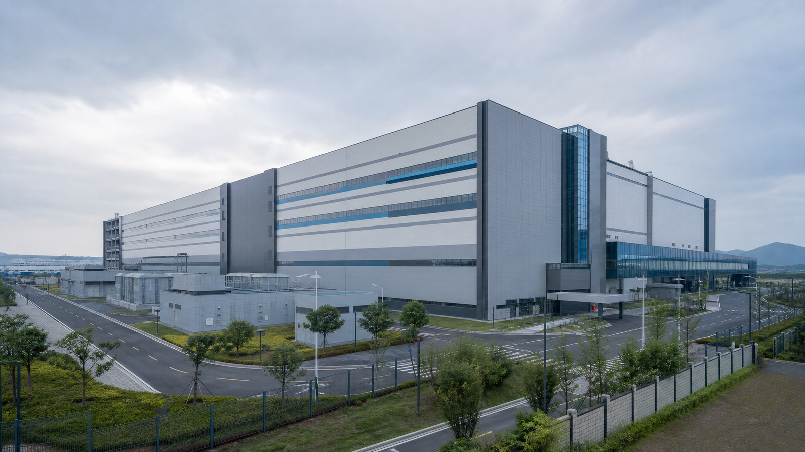
Kioxia’s reported rejection of an SK Hynix manufacturing tie-up suggests AI-era memory expansion may remain fragmented. Antitrust pressure and legacy joint-venture structures are still shaping investment paths.
-
Intel and ASML’s High NA EUV Milestone Carries Strategic Weight Beyond a Single Chip Program
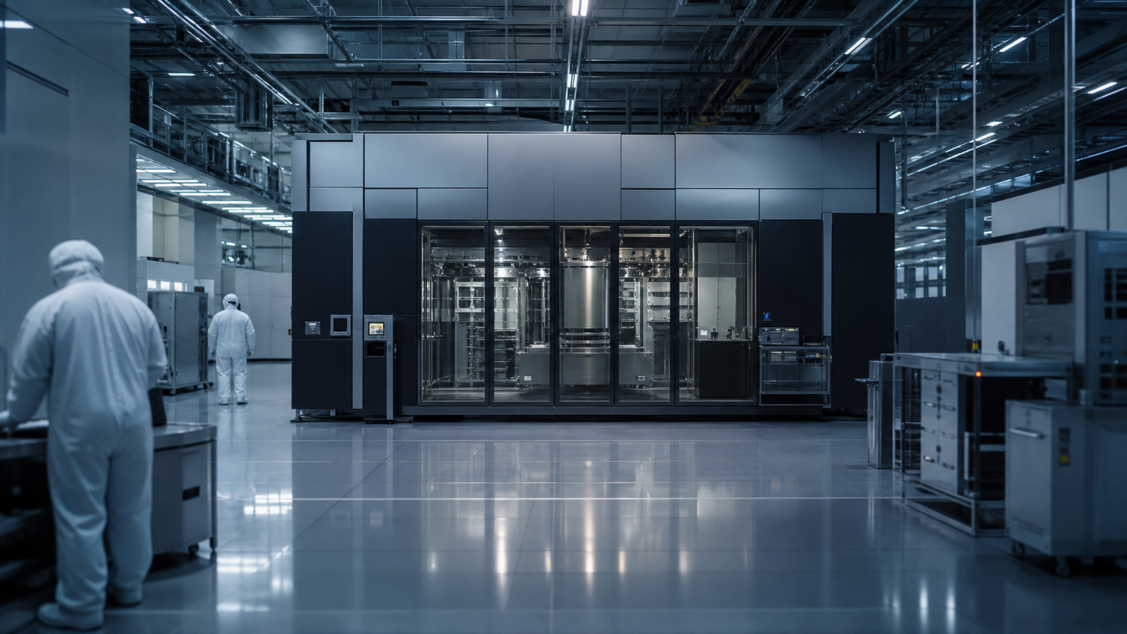
Intel and ASML’s reported High NA EUV milestone suggests next-generation lithography is moving from technical promise toward operational deployment. The shift could affect foundry strategy, equipment demand, and capital allocation across Asia.
-
Samsung and ASML Deepen Semiconductor Collaboration Around High NA EUV and Future DRAM
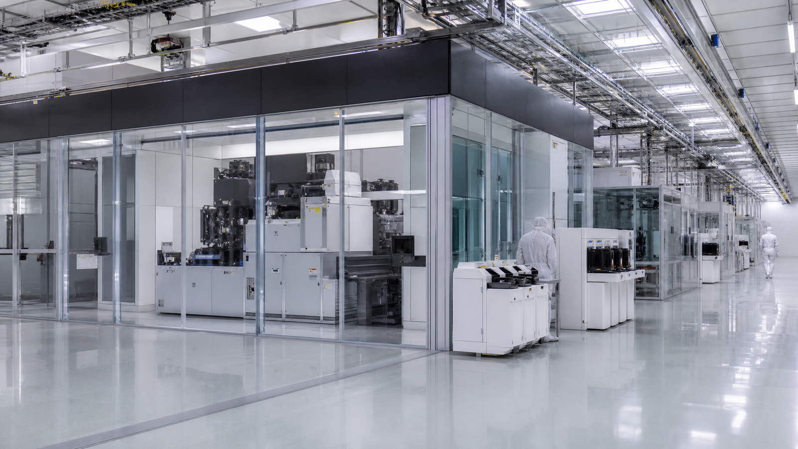
Samsung’s expanded ASML collaboration suggests next-generation lithography could move beyond logic and into future DRAM. The move points to tighter links between memory competitiveness, mask infrastructure, and frontier tooling, though timing and production impact remain unproven.
-
Nvidia’s $3.5 Billion MediaTek Bet: Keeping Custom AI Silicon Close to NVLink

Nvidia’s MediaTek investment may be less about financing and more about keeping custom AI silicon inside its broader system architecture. The move highlights a shift toward control of interconnect and rack-scale AI infrastructure.
-
TSMC’s Construction Surge Shows the Physical Limits of Scaling AI Chip Capacity
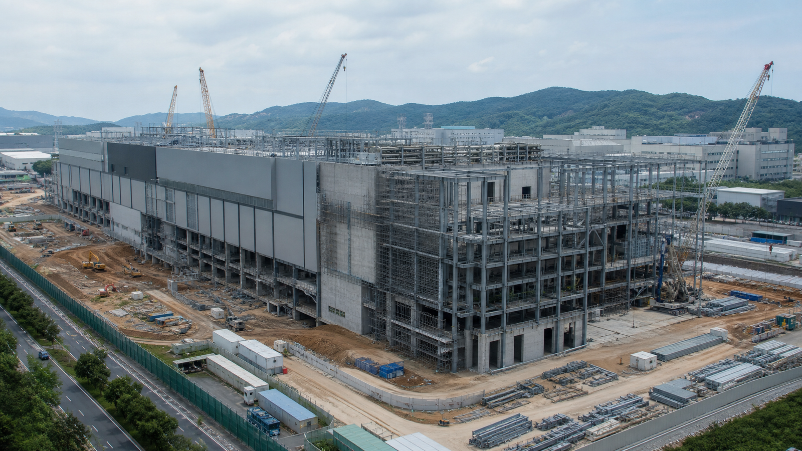
TSMC is building 25 fabrication and packaging facilities, yet it reportedly still cannot keep up with AI demand. The story points to construction labor and execution as the next constraint on semiconductor capacity.
-
TSMC Executive Signals AI’s Next Phase in Integrated Computing Systems
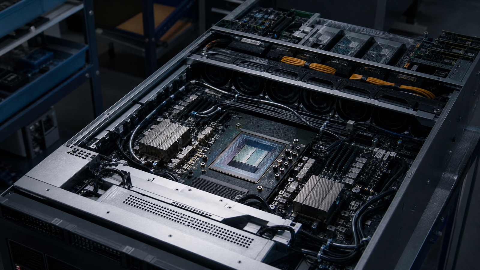
TSMC’s AI message points to a shift from chip performance to system integration. That raises the importance of packaging, memory, interconnect, and coordination across Asia’s supply chain.
-
TSMC’s Taichung 1.4nm Fab Moves Ahead of Schedule, Reinforcing Taiwan’s Advanced-Node Lead
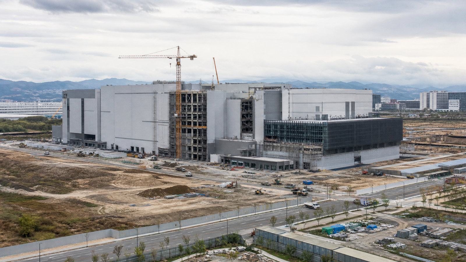
TSMC’s Taichung 1.4nm fab is moving ahead of schedule, reinforcing Taiwan’s role as the core base for next-generation chip capacity. The timeline supports confidence in future AI chip supply, but equipment, yields, and customer qualification remain the real tests.