Executive Summary
According to the available source information, Tata Electronics and Fujifilm have signed a memorandum of understanding to develop a semiconductor materials ecosystem around Tata Electronics’ Dholera fab project in Gujarat. The source summary says Fujifilm plans to invest Rs 800 crore, or about $83 million, in phases to build a materials plant in the Dholera Special Investment Region.
The announcement matters because semiconductor manufacturing is not sustained by fab construction alone. It also depends on reliable access to high-purity process materials that meet demanding quality standards. For India, which is trying to build semiconductor capacity and a broader electronics manufacturing base, the more important question may be whether upstream suppliers are willing to localize alongside new fabrication projects.
This does not by itself establish a fully formed domestic materials ecosystem. But it may signal a more serious effort to build one around Dholera rather than relying only on imported inputs. For TechPowerAsia readers, the development is relevant not just as a corporate partnership between an Indian and a Japanese company, but as an early test of whether India’s semiconductor strategy can expand from site-level fab ambition into cluster-level industrial execution.
Watch the Short Brief
Watch this short visual briefing for the key strategic implications behind the story.
Key Developments
– According to the source summary, Tata Electronics and Fujifilm signed an MoU to develop a semiconductor materials ecosystem linked to Tata’s Dholera fab project.
– The same source summary states that Fujifilm will invest Rs 800 crore, or roughly $83 million, in phases to establish a materials plant.
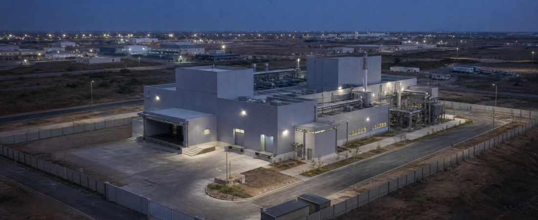
– The planned facility is expected to be located in the Dholera Special Investment Region in Gujarat.
– The reported objective is to support semiconductor materials localization around the Dholera project.
– The announcement connects two important Asian technology markets: India as an emerging semiconductor manufacturing location, and Japan as a longstanding supplier of critical semiconductor inputs and industrial know-how.
– The source material was published on September 17, 2026.
The available information does not specify the plant’s production start date, capacity, ownership structure, or the exact material categories to be manufactured. Those details will matter in assessing how meaningful the localization effort becomes in practice.
Strategic Analysis
The strategic value of this announcement lies less in the headline investment size than in what layer of the semiconductor stack it targets. New fab projects tend to attract most public attention because they are visible, capital intensive, and politically symbolic. But fabs operate within a much wider industrial system that includes materials, chemicals, equipment servicing, logistics, power stability, water treatment, and process control. If that supporting system remains underdeveloped, local fabrication capacity can still end up heavily dependent on imported inputs.
That is why the Tata-Fujifilm announcement deserves attention even though it is still early-stage. According to the reported information, this is not simply a customer-supplier arrangement involving imported materials. It points instead to a physical investment in India tied to a specific semiconductor geography: Dholera. If executed, that would make it more significant than a standard supply agreement, because it suggests an effort to build local manufacturing capability around the fab rather than around a distant downstream market.
In semiconductor manufacturing, proximity can matter. Many inputs require consistent quality, careful handling, and dependable delivery. A supplier located inside or near the same industrial region as a fab may reduce transport complexity and shorten response times if operational issues emerge. It can also improve coordination during qualification and ramp-up, though the available source information does not state how far this particular partnership will go in those areas.
For India, the broader issue is ecosystem formation. The country has spent years trying to move up the electronics value chain, but semiconductor manufacturing requires more than policy intent and land allocation. It requires supplier confidence. Foreign companies must decide whether demand will justify local production, whether infrastructure can support precision manufacturing, and whether fab timelines are credible enough to anchor upstream investment. A phased Rs 800 crore commitment from Fujifilm, as described in the source summary, may indicate that at least one established Japanese player sees enough strategic logic in Dholera to place an early bet.
That is meaningful because upstream localization is often harder than fab groundbreaking. A fab announcement can be made quickly; a functioning supply ecosystem takes much longer to build and requires multiple firms making interdependent commitments. One implication of the Tata-Fujifilm deal is that Dholera may be trying to position itself as more than a single-project semiconductor site. It may be aiming to become a cluster in which anchor manufacturing capacity gradually attracts adjacent suppliers.
This cluster logic matters across Asia. The region’s most durable semiconductor hubs did not develop through isolated investments alone. They became competitive because suppliers, manufacturing assets, technical labor, and infrastructure reinforced each other over time. India’s challenge is not only to launch projects, but to create enough follow-through that suppliers view local presence as commercially rational rather than politically encouraged but operationally risky.
The India-Japan dimension also stands out. Japan remains strategically important to the semiconductor supply chain through materials, equipment, and process-related capabilities. A Fujifilm investment in Dholera, if carried through as reported, would add substance to India-Japan industrial cooperation in a sector where execution depth matters more than diplomatic headlines. It may also show how Asian semiconductor partnerships are becoming more distributed: not necessarily replacing established hubs, but extending parts of the value chain into newer manufacturing geographies.
Still, scale should be kept in perspective. A single materials plant does not establish semiconductor self-sufficiency, and an MoU does not guarantee a mature supply network. The current announcement is better understood as a building-block event. Its importance depends on whether it leads to physical construction, successful qualification, and additional supplier participation around the same ecosystem.
There is also a timing issue embedded in the story. The economic logic of localized materials production depends heavily on the progress of the associated fab project. If the Dholera fab timeline advances steadily, upstream localization becomes easier to justify. If the fab faces delays, demand assumptions for adjacent suppliers could weaken. In that sense, the materials investment and the fab project should be viewed as linked execution tests rather than separate developments.
Investor Takeaway
For investors and industry observers, this announcement should be treated as an early but strategically relevant indicator of how India’s semiconductor buildout may evolve.
The first question is execution. The source summary says Fujifilm plans to invest in phases, which means the pace, sequencing, and eventual scope of that investment will matter more than the headline number alone. Investors should monitor whether the project moves from memorandum to construction, and whether additional operating details are disclosed.
The second question is ecosystem follow-through. One localized materials plant can support a narrative of intent, but it does not by itself create a resilient semiconductor cluster. The stronger signal would be follow-on commitments from other materials, process, or infrastructure suppliers in Dholera or nearby semiconductor zones.
The third question is demand visibility. The strategic value of the Fujifilm project is closely tied to Tata Electronics’ Dholera fab project. If the fab progresses, the supplier ecosystem case strengthens. If timelines slip materially, the investment thesis around local supporting capacity becomes less clear.
The fourth question is whether India-Japan cooperation in semiconductors starts to deepen at the operating level. This announcement may be an important first marker, but investors should watch for additional joint activity, capital commitments, or ecosystem partnerships before drawing broader conclusions.
The core takeaway is that this is a supply-chain story as much as a manufacturing story. According to the available source information, Fujifilm is not just supplying from abroad; it is planning a local industrial footprint around Dholera. If that footprint is built and matched by further ecosystem investment, it could improve the credibility of India’s semiconductor ambitions. If it remains a one-off project without wider follow-through, its strategic significance will be narrower.
For now, the announcement is best read as a cautious positive signal: a sign that some upstream confidence may be forming around India’s semiconductor push, but not yet proof that a self-sustaining materials ecosystem has arrived.