Executive Summary
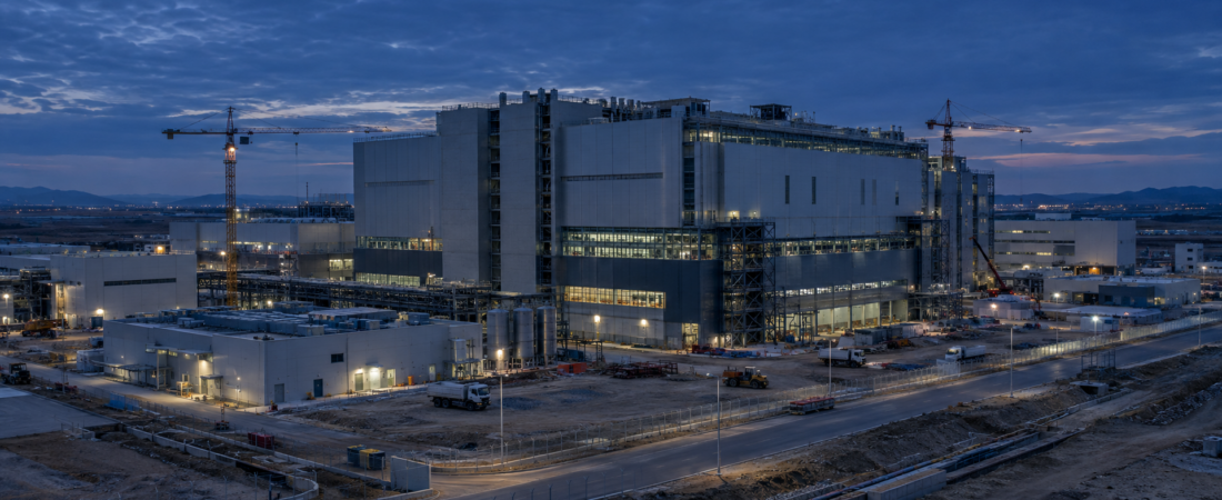
According to the reported information, Tata Electronics has partnered with Malaysia-based Kelington to provide critical infrastructure, systems integration, and tool hook-up services for Tata’s commercial semiconductor fab in Dholera, Gujarat. The project is described as an $11 billion facility and stands out as one of India’s highest-profile attempts to establish domestic semiconductor manufacturing capacity.
The announcement matters less as a new investment headline than as a signal that the project is moving deeper into the execution stage. In semiconductor manufacturing, tool hook-up, cleanroom-related infrastructure, and systems integration are among the most complex parts of a fab build. They sit close to the point where capital spending must translate into operational readiness.
For TechPowerAsia readers, the broader relevance is regional. The partnership links India’s semiconductor ambitions with Malaysian engineering capability, underscoring how Asia’s chip supply chain is not defined only by foundries and equipment vendors, but also by specialist infrastructure firms that make fabs usable. One strategic implication is that India’s semiconductor push may depend, at least in part, on imported execution expertise while local capabilities are still developing.
Watch the Short Brief
Watch this short visual briefing for the key strategic implications behind the story.
Key Developments
Tata Electronics has engaged Kelington, a Malaysian engineering firm, to support the Dholera fab project in Gujarat.
According to the available source information, Kelington’s role includes critical infrastructure, systems integration, and tool hook-up services. These are core enabling functions in semiconductor fab construction, particularly in the late build and installation phases.
The Dholera project is described in the report as an $11 billion commercial semiconductor fab. Beyond that, the available information does not establish additional technical details such as wafer format, capacity, process node, equipment suppliers, or timing for operational launch.
The cross-border element is notable. Tata Electronics represents one of India’s flagship semiconductor efforts, while Kelington brings engineering expertise from Malaysia, a country with long-standing participation in the regional semiconductor ecosystem.
At the same time, several points remain outside the confirmed record available here. The report summary does not specify contract value, completion milestones, the full scope of Kelington’s responsibilities inside the project, or whether other major engineering and integration partners are working alongside it.
Strategic Analysis
The most important takeaway is that India’s semiconductor strategy is being tested less by policy design than by industrial execution. Large fab projects do not succeed on headline investment figures alone. They depend on highly specialized workstreams that connect buildings, utilities, contamination control, and process tools into a functioning production environment. The reported Tata-Kelington arrangement suggests that Dholera is moving into that execution-heavy phase.
That matters because semiconductor fabs are unusually unforgiving infrastructure projects. Tool hook-up and systems integration require precision coordination across power, gases, chemicals, water, air handling, vibration control, and cleanroom standards. Even when financing and policy support are in place, these late-stage construction and installation processes can become bottlenecks. For India, the strategic question is not only whether capital has been committed, but whether execution quality can hold schedule and technical integrity through commissioning.
Kelington’s involvement also highlights a broader Asian supply-chain reality. Semiconductor capacity expansion depends on a network of specialist firms that often receive less attention than chipmakers or tool vendors. Malaysia has built a durable role in that network over decades, and the Tata-Kelington partnership may indicate that India is drawing on established Southeast Asian expertise to bridge domestic capability gaps.
That should not automatically be read as a weakness. Cross-border engineering dependence is common in semiconductors, including in mature markets. The more important issue is whether such dependence remains transitional or becomes structural. If India’s fab ambitions expand over time, it will likely need not only capital and incentives, but also a deeper domestic base of cleanroom engineering, facilities integration, and semiconductor-construction talent. Without that, future projects could face repeated reliance on a relatively narrow regional pool of specialists.
This is where the Asia relevance becomes particularly strong. The semiconductor race across the region is often framed around fabrication capacity, advanced packaging, export controls, or industrial policy. But another constraint is emerging in parallel: the availability of firms that can physically deliver and integrate highly complex production environments. As more governments and conglomerates pursue semiconductor localization, these engineering specialists may become a competitive choke point of their own.
In that sense, the Tata-Kelington partnership may be read as part of a larger reconfiguration of regional capability flows. India brings market scale, policy ambition, and corporate backing. Malaysia brings specialized execution experience. The result is not simply a vendor contract; it is an example of how Asia’s semiconductor ecosystem is increasingly being assembled through cross-border capability sharing rather than purely national supply chains.
There is also a signaling effect. Dholera has become one of the most visible tests of whether India can move from semiconductor aspiration to operational manufacturing. A reported partnership focused on infrastructure and tool integration suggests that the conversation is shifting from announcement politics toward industrial delivery. That does not guarantee success, and it does not on its own validate broader claims about India’s long-term semiconductor competitiveness. But it does point to a more concrete phase of development.
The main risk is execution concentration. Because the project is so visible, setbacks in areas such as facilities readiness, tool installation, or commissioning could shape perceptions far beyond one site. Fairly or not, delays at Dholera could influence external confidence in India’s wider semiconductor rollout, including adjacent investment narratives in materials, support services, downstream electronics manufacturing, and future fab proposals.
At the same time, observers should avoid over-reading a single contract. The available information supports the conclusion that progress is being made on execution-related work. It does not yet establish how fast the fab is advancing, when tools will be fully installed, or how smoothly the site will move toward commercial operation. The strategic significance is real, but it remains tied to follow-through.
Investor Takeaway
The reported Tata-Kelington partnership is best treated as an execution milestone rather than a stand-alone market catalyst. It adds evidence that the Dholera fab is progressing into a technically demanding build phase, where infrastructure integration becomes central to project credibility.
For investors and strategic industry watchers, several issues now matter more than the announcement itself.
First, monitor whether the project produces visible follow-on milestones. Updates related to infrastructure completion, cleanroom readiness, tool arrival, installation, or commissioning would offer stronger signals about execution quality than the initial partnership disclosure.
Second, watch whether Kelington’s role remains isolated to Dholera or becomes part of a broader pattern in India. If more fab or semiconductor infrastructure projects in India turn to Southeast Asian engineering specialists, that would suggest a structural regional dependency rather than a one-off contracting decision.
Third, track whether India’s semiconductor ecosystem begins building more local execution depth around fab construction and systems integration. One long-term measure of success will be whether domestic capabilities expand alongside physical assets.
Fourth, keep the supply-chain lens wide. Specialist engineering firms are becoming increasingly important in Asia’s semiconductor buildout. Their availability, capacity, and geographic positioning may influence how quickly new manufacturing projects can move from approved capital plans to real output.
The bottom line is that this development strengthens the case that India’s semiconductor effort is entering a more operational phase. But the real test now shifts to delivery. For Dholera, and by extension for India’s broader semiconductor credibility, infrastructure execution may matter as much as strategy, funding, or political intent.