Executive Summary
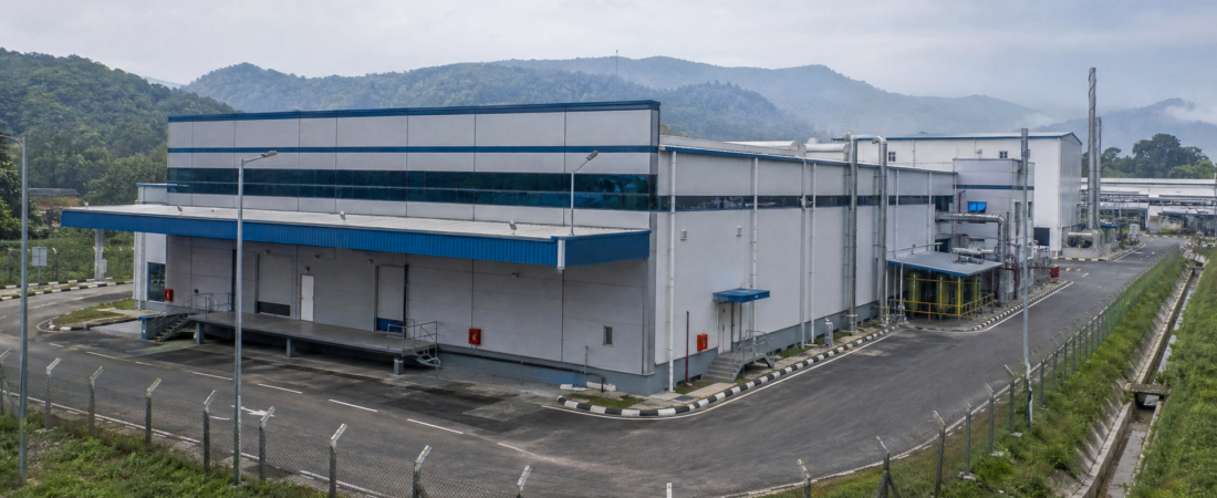
Tata Electronics has signed a memorandum of understanding with Dutch semiconductor assembly equipment specialist BE Semiconductor Industries, or Besi, in connection with Tata’s semiconductor packaging facility in Jagiroad, Assam. According to the available source information, the partnership is intended to leverage Besi’s advanced packaging equipment and technologies for the $3 billion site.
On its face, this is a straightforward supplier-partner announcement. Strategically, however, it points to a larger shift in how new semiconductor hubs are being built. For emerging manufacturing locations, packaging capability is no longer just a lower-value back-end function. It is increasingly tied to performance, system integration, and the ability to participate in higher-end parts of the semiconductor value chain as AI and heterogeneous computing workloads expand.
For India, the reported Tata-Besi tie-up may indicate a pragmatic route into this segment: combine large domestic capital commitments with imported equipment and process support from established global specialists. That approach could accelerate capability build-out, but it also underscores a structural reality. New entrants may be able to localize facilities faster than they can localize the equipment ecosystem that makes those facilities competitive.
The key question is not only whether India can add packaging capacity, but whether it can sustain technology access, ramp execution, and customer credibility over time.
Watch the Short Brief
Watch this short visual briefing for the key strategic implications behind the story.
Key Developments
According to the source summary, Tata Electronics and Besi have signed an MoU tied to Tata’s $3 billion semiconductor packaging facility in Jagiroad, Assam.
The available source information indicates that Tata plans to use Besi’s advanced packaging equipment and technologies at the site. No further detail was provided on equipment types, packaging formats, production capacity, or deployment timing.
Besi is a Netherlands-based specialist in semiconductor assembly equipment. The reported partnership therefore links an Indian semiconductor manufacturing project with European equipment capability, reinforcing the cross-border nature of the build-out.
The announcement appears to come from Tata Electronics’ own published communication. That matters because it supports the existence of the partnership, but it also means readers should treat the disclosure primarily as a company-announced strategic step rather than as evidence of completed installation, production readiness, or customer qualification.
The available information does not specify the commercial value of the MoU, whether the arrangement is exclusive, or how much of the Assam facility’s future packaging line-up will depend on Besi equipment.
Strategic Analysis
This development is best understood as part of a broader revaluation of advanced packaging within the semiconductor stack. For years, front-end wafer fabrication drew most of the strategic and financial attention, while packaging was often treated as a lower-profile segment. That balance has been changing. As chip designers seek more performance through integration, packaging becomes more central to product architecture rather than simply a finishing step.
That shift matters especially in Asia, where semiconductor geography is being reconsidered in response to industrial policy, supply-chain resilience concerns, and AI infrastructure demand. New semiconductor locations do not need to replicate the entire fabrication ecosystem immediately to become relevant. Packaging can offer a more accessible entry point. But “more accessible” does not mean easy. Advanced packaging still relies on specialized tools, process know-how, and tight execution discipline.
In that context, the Tata-Besi MoU may signal how India is approaching the problem. Rather than waiting for a fully domestic equipment base to emerge, the near-term strategy appears to rely on partnerships with established global suppliers. That is a rational path if the objective is to shorten time to capability. It aligns with the reality that much of the packaging toolchain remains concentrated among a relatively small group of international equipment providers.
One implication is that semiconductor localization and semiconductor sovereignty are not the same thing. A country may host capital-intensive facilities and still remain dependent on external partners for core process tools, upgrades, spare parts, and technical support. The Assam project, if it progresses as intended, could therefore expand India’s role in the semiconductor supply chain while still leaving it exposed to external equipment dependencies.
That does not weaken the significance of the project. It clarifies its strategic logic. For a market trying to move from ambition to execution, supplier relationships are often the first proof point that a facility is more than a policy headline. Equipment access is what turns capex announcements into operational possibility.
The India-Netherlands dimension is also worth noting. Semiconductor supply chains increasingly span multiple policy jurisdictions even when manufacturing is framed in national terms. A partnership between Tata Electronics and Besi highlights how capacity creation in South Asia remains tied to specialized expertise in Europe. For investors and industry observers, this is a reminder that semiconductor diversification rarely means self-contained local ecosystems in the early stages. It usually means new combinations of geography and dependency.
This has broader implications for Asia’s packaging landscape. If India can build credible packaging operations with support from global equipment partners, it could strengthen its position in the region’s semiconductor map without first competing head-on in leading-edge wafer fabrication. That possibility may be particularly relevant as governments and companies look for ways to distribute manufacturing risk more widely across Asia.
At the same time, the announcement should not be read as proof that India has already solved the harder part of the equation. Facility construction, equipment procurement, process integration, workforce training, yield ramp, and customer acceptance are all distinct hurdles. The available source information confirms the partnership intent, but not the outcome. In semiconductor manufacturing, the gap between announced capability and demonstrated capability can be significant.
The most useful reading, then, is disciplined rather than celebratory. The MoU is an enabling signal. It suggests Tata Electronics is assembling the supplier relationships needed to support a serious packaging effort in Assam. But the ultimate strategic value will depend on whether those relationships translate into reliable operations and commercially relevant output.
Investor Takeaway
For investors tracking semiconductor equipment, Asian manufacturing expansion, and India’s industrial technology ambitions, this announcement is meaningful as an early execution indicator rather than a finished milestone.
Three points stand out.
First, equipment access is becoming a more visible differentiator in new semiconductor projects. The reported Tata-Besi partnership suggests that advanced packaging build-outs will be shaped not just by capital deployment, but by which suppliers are willing and able to engage with new geographic entrants.
Second, India’s semiconductor push may be gaining substance through targeted partnerships rather than broad ecosystem completeness. That can be an effective model in the near term, but it also means operational progress will likely depend on continued access to foreign equipment and technical support.
Third, the announcement reinforces the strategic importance of the packaging layer across Asia. If more countries pursue semiconductor entry through back-end manufacturing and advanced packaging, competition for specialized tools, engineering talent, and customer trust could intensify.
The practical signals to monitor next are straightforward: confirmation of equipment deployment milestones, additional supplier relationships, clearer disclosure on the Assam facility’s operating scope, and any evidence that the site is moving from construction-phase planning toward commercial readiness. Investors should also watch whether Tata Electronics frames future updates around process capability and ecosystem partnerships, not just project scale.
In short, the Tata-Besi MoU is best viewed as a credible step in India’s semiconductor build-out, with the strongest significance lying in what it says about packaging strategy, supplier dependency, and Asia’s evolving semiconductor geography. The partnership matters today as a directional indicator. Its lasting importance will depend on execution.