Executive Summary
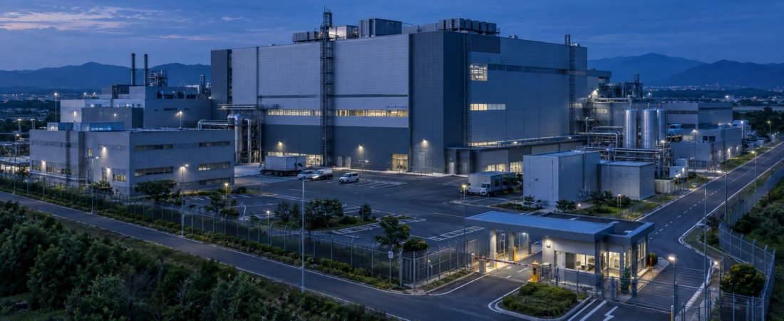
Japan’s Ministry of Economy, Trade and Industry has approved TSMC’s revised plan to manufacture 3nm logic chips at its second Kumamoto fab, according to the available source information. That approval qualifies the expansion for up to $4.1 billion in state subsidies.
The reported decision matters because it suggests Japan is prepared to support a more advanced level of semiconductor manufacturing onshore than many recent overseas capacity deals have involved. For TSMC, the move may also reflect the growing importance of government-backed capital support in determining where future chip capacity is built.
For TechPowerAsia readers, the significance is less about a single subsidy figure and more about what it may signal for Asia’s semiconductor map. Japan is using industrial policy to deepen its role in strategic chip manufacturing, while Taiwan’s most important foundry appears willing to broaden its manufacturing footprint in allied markets when policy support is strong enough.
Much remains unconfirmed, including production timing, output scale, and the exact commercial structure around the fab. Even so, the reported approval is an important marker for Japan-Taiwan technology cooperation, state-backed semiconductor competition, and the broader question of how advanced capacity is being distributed across Asia.
Watch the Short Brief
Watch this short visual briefing for the key strategic implications behind the story.
Key Developments
– METI has approved TSMC’s revised plan to produce 3nm logic chips at its second Kumamoto fab, according to the source summary.
– The project now qualifies for up to $4.1 billion in Japanese state subsidies, based on the same source information.
– The report was published on October 17, 2026.
– The available source information identifies Japan and Taiwan as the key regions in this development, underscoring the cross-border nature of the project.
– Sony and Denso are listed as related companies in the source package, but the available information does not confirm a direct role for either company in this specific 3nm expansion.
– The source summary does not provide details on capacity, construction schedules, equipment installation, production start dates, customer commitments, or employment impact.
At a minimum, the reported approval indicates that Tokyo is willing to put substantial financial support behind semiconductor manufacturing tied to an advanced logic node. It also indicates that TSMC’s Kumamoto plans have moved beyond a generic expansion narrative into a more strategically significant manufacturing proposal.
Strategic Analysis
The most immediate implication of the reported approval is that Japan’s semiconductor policy is becoming more targeted and more ambitious in technological scope. Subsidies for chip manufacturing are no longer just about adding volume or supporting industrial resilience in broad terms. In this case, according to the report, the policy support is linked to 3nm logic production, which places the discussion firmly in the advanced manufacturing category.
That matters for Asia because the region’s semiconductor competition is increasingly being shaped by a mix of public funding, strategic alignment, and supply-chain risk management. Governments are not only trying to attract fabs; they are trying to attract the right kinds of fabs. If the reported Kumamoto plan proceeds as described, Japan would strengthen its position in a part of the semiconductor value chain that carries both economic and geopolitical weight.
For TSMC, the reported approval may indicate how central government incentives have become to fab location decisions. Advanced semiconductor capacity is expensive, operationally complex, and politically sensitive. In that environment, large-scale subsidy support can alter the economics of cross-border expansion. One strategic implication is that public co-funding is becoming a more decisive factor in capital allocation for advanced chip production, particularly in markets seeking a larger role in trusted supply chains.
The Japan-Taiwan dimension is also important. TSMC remains the anchor of Taiwan’s semiconductor strength, while Japan brings policy support, industrial depth, and a major customer base across electronics, automotive, and manufacturing sectors. The reported Kumamoto approval therefore points to a deeper form of regional technology interdependence: Taiwan-based process leadership paired with Japanese state support and local industrial infrastructure.
That does not automatically mean a rapid or broad relocation of advanced chipmaking across the region. The available source information is too limited to support stronger conclusions about scale, pace, or strategic priority relative to TSMC’s other global projects. But it does suggest that Japan is competing for a more meaningful role in future semiconductor capacity rather than limiting itself to supporting adjacent parts of the supply chain.
The subsidy figure itself is strategically revealing. Up to $4.1 billion is large enough to reinforce a broader industry pattern: governments are increasingly willing to absorb part of the cost of semiconductor expansion in exchange for domestic manufacturing presence. This is especially relevant in Asia, where semiconductor policy is now tied not only to economic growth but also to technology sovereignty, supply security, and alliance-building.
There is also a signal here for other regional governments. If Japan can secure support for a 3nm manufacturing plan through a combination of industrial policy and partnership with TSMC, peer economies may feel pressure to sharpen their own incentives, infrastructure offers, and permitting frameworks. The result could be a more competitive regional environment for attracting advanced-node investment.
Sony and Denso should be treated carefully in this context. They are identified as related companies in the source package, but the available information does not establish them as confirmed partners, customers, or co-investors in this specific 3nm expansion. Even so, their presence in the broader Kumamoto ecosystem highlights a recurring feature of semiconductor industrial policy in Asia: governments often try to build local manufacturing clusters around a major anchor investor, with downstream benefits for domestic industry if the ecosystem develops successfully.
The key strategic uncertainty is execution. Subsidy approval is important, but it is only one stage in turning an advanced-node project into real output. Investors and industry observers still need confirmation on timelines, equipment deployment, workforce readiness, and customer demand. In semiconductor manufacturing, especially at advanced nodes, political intent and commercial reality do not always move at the same speed.
Investor Takeaway
For investors, the reported Kumamoto approval is best read as a policy and capital-allocation signal rather than a fully defined production event. The confirmed core point is narrow but important: Japan has approved TSMC’s revised 3nm plan for its second Kumamoto fab, and the project now qualifies for up to $4.1 billion in support according to the source.
What matters next is whether that approval translates into visible project milestones. Investors should monitor four areas in particular.
First, watch for clarity on timing. Construction progress, equipment delivery schedules, and production targets will determine whether the project is merely policy-positive or also commercially meaningful on a reasonable timeframe.
Second, watch for detail on scale. The source summary does not disclose planned output levels, which means the market still lacks a clear view on how material this facility could become within TSMC’s broader manufacturing network.
Third, monitor ecosystem signals inside Japan. That includes whether domestic industrial groups, suppliers, or technology customers publicly align with the project over time. Sony and Denso are relevant names to track because they are associated with the broader story, but their roles in this specific 3nm plan remain unconfirmed in the available information.
Fourth, place the development in the context of Asian semiconductor policy competition. If this project advances smoothly, it may reinforce the case that large state incentives can influence where strategically important capacity is built. That would have implications not only for foundries, but also for equipment vendors, materials suppliers, industrial real estate, and power and infrastructure providers connected to semiconductor expansion.
The central risk is that investors may overread the approval before more operational details emerge. Subsidy qualification is not the same as proven ramp, and a reported 3nm plan is not yet evidence of commercial scale or customer concentration. Still, as a directional signal, the move is significant. It suggests Japan intends to stay active in the competition for advanced semiconductor relevance, and it highlights how cross-border semiconductor strategy in Asia is increasingly being shaped by the interaction of state funding, industrial alignment, and long-horizon capacity planning.