Article Title
Samsung Weighs Foundry Pivot for 2nm HBM Base Dies in Bid for Future NVIDIA Demand
Executive Summary
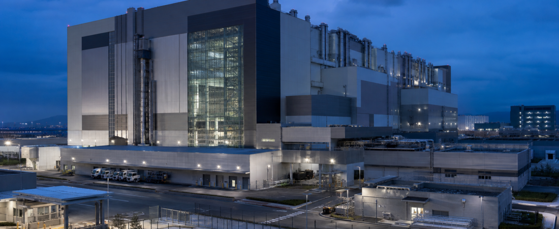
Samsung Electronics is reportedly considering a meaningful change to its semiconductor manufacturing plan in South Korea. According to the available source information, the company may repurpose its NRD-K Line 2 facility in Giheung, which was originally planned for research and development, into a foundry production line for mass-producing 2nm base dies for next-generation high-bandwidth memory.
The reported objective is strategically important: positioning Samsung to secure future NVIDIA demand tied to advanced AI hardware. While the available information does not indicate a confirmed customer commitment, the possibility alone highlights how deeply AI infrastructure demand is now influencing capital allocation across Asia’s semiconductor supply chain.
For TechPowerAsia readers, the significance goes beyond a single factory decision. If accurate, the reported move would underscore a broader shift in the memory market: high-bandwidth memory is increasingly tied not only to DRAM stacking and packaging capability, but also to access to advanced logic manufacturing. That raises the strategic value of integrated chipmakers that can connect memory, logic, and packaging capabilities inside one regional production ecosystem.
Just as importantly, this remains a reported consideration rather than a confirmed final decision. Investors should read it as an early signal about Samsung’s priorities in AI semiconductors, not as proof that new production capacity or NVIDIA orders are already locked in.
Watch the Short Brief
Watch this short visual briefing for the key strategic implications behind the story.
Key Developments
According to the report, Samsung is considering converting its NRD-K Line 2 facility in Giheung, South Korea, from an R&D-focused line into a foundry production line.
The reported production target is 2nm base dies for next-generation HBM products. These base dies sit beneath stacked memory and are becoming increasingly important in AI-oriented memory architectures.
The source summary indicates that Samsung’s motivation is to improve its chances of securing future NVIDIA business. The available information does not confirm an order, supply agreement, production schedule, or volume commitment.
What is confirmed from the source package is limited but important: the companies involved are Samsung Electronics and NVIDIA, the reported geography is South Korea, and the publication date is August 14, 2026.
The source information does not provide specific details on capital expenditure, output capacity, equipment changes, expected start dates, or whether Samsung has made a final internal decision. Those missing details matter because they would determine whether this is a tactical adjustment or part of a larger repositioning of Samsung’s foundry and memory strategy.
Strategic Analysis
If confirmed, the reported line conversion would illustrate one of the most important structural changes in the AI chip supply chain: the boundary between memory manufacturing and advanced logic manufacturing is becoming less distinct.
HBM has become a critical component in AI accelerators because it helps feed large amounts of data to high-performance processors. As HBM evolves, the base die underneath the memory stack can become more strategically significant. That changes the competitive equation. A company is no longer competing only on memory density, stacking skill, and packaging quality; it may also need credible access to leading-edge logic process technology.
That is why this report matters for Samsung in particular. Samsung is one of the few semiconductor companies with meaningful positions in both memory and foundry. If it redirects an R&D-designated line toward commercial foundry production for 2nm HBM base dies, the move could indicate an effort to use that integrated structure more aggressively in pursuit of AI-related demand.
One implication is that Samsung may be trying to tighten the link between its memory business and its advanced process ambitions. In the AI hardware market, the value is increasingly concentrated not just in standalone chips, but in tightly coordinated platforms that combine compute, memory, packaging, and manufacturing reliability. A successful 2nm HBM base die strategy could strengthen Samsung’s role in that stack.
Another implication concerns timing. Repurposing a line originally planned for R&D, if that is what ultimately happens, could suggest that Samsung sees a market window worth pursuing sooner rather than later. That does not necessarily mean the company faces immediate pressure, but it may indicate that internal manufacturing flexibility is being weighed against commercial opportunity.
There is also a trade-off embedded in the reported plan. R&D lines support future process development, experimentation, and learning cycles. Production lines support near-term revenue opportunities and customer capture. If Samsung shifts resources from one to the other, the company may be balancing long-range technology development against the near-term strategic importance of winning business in the AI supply chain. Whether that trade-off proves effective would depend on execution, timing, and actual customer demand.
The Asia relevance is direct. South Korea already holds a central role in the global memory industry, while East Asia more broadly remains the core manufacturing base for advanced semiconductors. A reported Samsung move to align South Korean foundry capacity with next-generation HBM demand would reinforce the region’s importance in the AI hardware stack.
It also points to a larger competitive pattern across Asia. The AI buildout is driving tighter integration between different parts of the semiconductor value chain: memory, foundry, advanced packaging, and supply-chain orchestration. Companies that can coordinate these layers effectively may improve their standing with major AI platform customers. Companies that cannot may find that strength in one segment is no longer enough.
NVIDIA’s role in the report is especially notable. Even without a confirmed order, the fact that future NVIDIA demand is cited as a strategic target shows how concentrated influence has become in AI semiconductors. A small number of end-market platforms can shape investment priorities far upstream, affecting fab planning, process-node deployment, and supplier positioning across Asia.
That concentration creates opportunity but also risk. For Samsung, winning future AI-related business could improve utilization and strengthen its strategic relevance in the advanced memory ecosystem. But a strategy oriented around one dominant demand center can also increase exposure to qualification delays, technology transitions, and shifts in customer sourcing strategy.
From a capital-allocation perspective, the reported possibility is a useful signal because it suggests that advanced-node capacity decisions are no longer being driven only by traditional foundry logic demand. AI memory subsystems are now important enough to influence where and how some next-generation manufacturing capacity may be deployed. That is a meaningful change for how investors should think about semiconductor capex in the region.
Investor Takeaway
The most important point is discipline around what is known and what is not. What is known is that a report says Samsung is considering repurposing an R&D-oriented facility in Giheung into a foundry line for 2nm HBM base dies, with the aim of targeting future NVIDIA demand. What is not known is whether Samsung has made a final decision, how large the investment would be, when any line would become operational, or whether customer commitments already exist.
Even so, the reported development deserves attention because it may signal how the AI semiconductor race is changing capacity priorities in Asia. Investors should monitor whether Samsung formally confirms the line conversion, whether management commentary starts linking foundry strategy more closely to HBM opportunity, and whether future disclosures provide evidence of node-specific capacity being aligned with AI memory demand.
A second area to watch is whether Samsung can translate its integrated structure into a clearer market proposition. The strategic case for combining advanced memory and logic capabilities is becoming stronger, but execution remains the real test. Converting strategic logic into commercially meaningful orders requires process maturity, manufacturing reliability, and customer confidence.
A third issue is regional significance. If South Korea-based capacity is increasingly configured around advanced AI memory components, that would further strengthen the country’s role in the global AI hardware supply chain. It would also reinforce Asia’s central position in the competition to support next-generation AI infrastructure.
In practical terms, this is best viewed as an early strategic indicator. If the report proves accurate, Samsung may be signaling that 2nm-era HBM base dies are important enough to justify reallocating manufacturing plans. If the move does not materialize, the report still highlights where competitive pressure is building: at the intersection of memory leadership, advanced-node access, and customer capture in AI systems.
For investors, the key question is not simply whether one line gets converted. It is whether Samsung can use its South Korean manufacturing base to become more deeply embedded in the next phase of the AI semiconductor stack.