Executive Summary
Taiwanese semiconductor equipment maker Skytech expects high demand to continue through the second quarter of 2027, according to the available source information. The reported strength is tied to the company’s physical vapor deposition equipment for panel-level packaging, an advanced packaging approach that is drawing traction with server and US customers.
The immediate significance is not that panel-level packaging has already become the industry standard for AI chips. The available information does not support that conclusion. Rather, Skytech’s outlook offers an early signal that parts of the semiconductor equipment chain in Taiwan are positioning around potential alternatives or complements to existing advanced packaging flows as AI hardware requirements grow.
For TechPowerAsia readers, the development matters because advanced packaging has become one of the most closely watched constraints in AI semiconductor scaling. If equipment demand around newer packaging formats continues to build, Taiwan’s role in AI infrastructure could deepen beyond foundry and assembly leadership into a more influential position in the upstream equipment layer.
Watch the Short Brief
Watch this short visual briefing for the key strategic implications behind the story.
Key Developments
Skytech, a Taiwanese semiconductor equipment maker, said demand is expected to remain high through Q2 2027, according to the report.
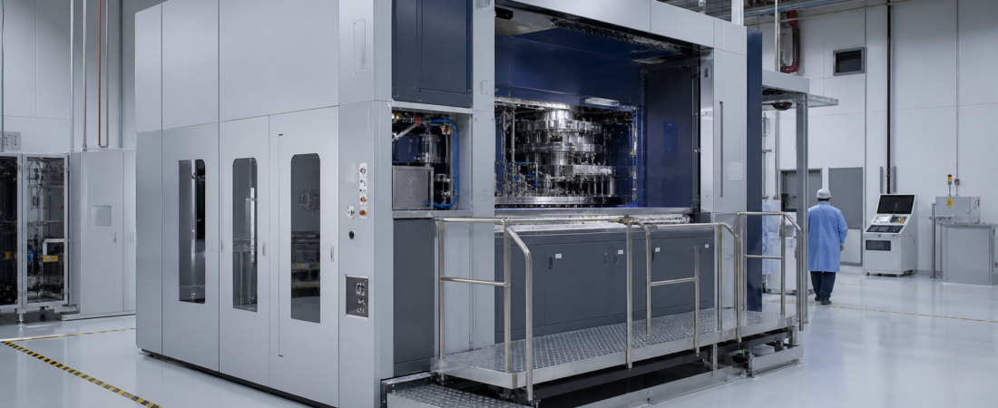
The demand outlook is linked to the company’s physical vapor deposition, or PVD, tools for panel-level packaging, or PLP.
According to the source summary, Skytech’s PLP-related equipment is gaining traction with server and US customers. The available information does not identify those customers or specify the scale of their programs.
This matters in the context of AI semiconductor production because advanced packaging has become a strategically important part of the hardware stack. AI accelerators increasingly depend on sophisticated packaging methods to integrate computing dies, memory, and interconnect structures into high-performance modules.
The broader Taiwan context is also important. Taiwan already occupies a central position in the semiconductor value chain through companies including TSMC in foundry manufacturing and ASE Technology in semiconductor assembly and testing. Skytech’s reported momentum points to potential activity in another layer of that ecosystem: packaging equipment.
At this stage, however, the reported development should be understood as a company-level signal rather than evidence of broad industry adoption. The source information supports Skytech’s demand outlook and customer traction, but it does not confirm a market-wide transition in packaging architecture.
Strategic Analysis
The strategic value of this story lies in what it may indicate about the next phase of AI chip scaling in Asia’s semiconductor supply chain.
For much of the current AI buildout, the market’s attention has centered on leading-edge logic production and high-bandwidth memory. But advanced packaging has increasingly become just as important. Even when computing dies are available, packaging capacity can still shape how quickly complete AI systems reach market. That makes any early shift in packaging equipment demand worth watching, especially in Taiwan, where major parts of the semiconductor manufacturing chain remain concentrated.
Skytech’s reported traction in PLP-related PVD equipment may suggest that some customers are exploring packaging approaches designed to support larger or more cost-sensitive high-performance applications. Panel-level packaging has long been discussed in the industry as a possible route to improve manufacturing efficiency versus strictly wafer-based approaches. The appeal, in theory, is that panel-based processing could offer better area utilization and potentially different cost and throughput characteristics.
Still, the key point is discipline: potential does not equal deployment at scale. The available source information does not establish that PLP is replacing established AI packaging flows today. Nor does it show that major foundries or outsourced semiconductor assembly and test providers have committed to a broad PLP roadmap. The more appropriate interpretation is that equipment demand around PLP is becoming visible enough to merit serious monitoring.
That distinction matters because advanced packaging transitions typically unfold slowly. New process flows must pass validation, yield improvement, customer qualification, and production integration. In semiconductors, technical promise often arrives well before commercial scale. A company statement about strong demand can be strategically useful, but it is not the same as confirmed industry migration.
Even so, the signal is relevant for three reasons.
First, it points to a possible expansion of where bottleneck relief may come from in AI hardware. Much of the conversation around AI semiconductor constraints has focused on capacity additions within existing packaging methods. If more customers begin to evaluate or adopt alternative packaging formats, then future capacity expansion may depend not only on more installed tools within current lines, but also on new categories of packaging equipment. That would create a different set of winners, dependencies, and capital spending priorities across the supply chain.
Second, the mention of server and US customers suggests that demand may be linked to the broader buildout of AI infrastructure rather than only to local or experimental programs. That does not confirm a large commercial ramp, and the customer names are not disclosed. But it does indicate that interest in packaging equipment tied to AI workloads is not confined to one narrow part of the market. If accurate, that could make Taiwan-based equipment suppliers more relevant to global data center and accelerator deployment timelines.
Third, the development reinforces Taiwan’s strategic depth. The island’s importance to AI hardware is usually framed through foundry output and OSAT capability. Skytech’s reported momentum hints at a broader industrial reality: Taiwan may also have leverage in the specialized equipment layer that supports how packaging technology evolves. If that layer becomes more important, Taiwan’s role in AI supply chains could become even harder to replicate quickly.
This is where ecosystem context matters. TSMC and ASE Technology remain central reference points because they represent Taiwan’s established strength in chip manufacturing and advanced packaging services. But the available information does not indicate any direct commercial relationship between those companies and Skytech in this case. Their relevance is structural, not transactional. Any sustained increase in demand for PLP-related tools would matter partly because it would emerge inside a market already anchored by those larger Taiwanese capabilities.
There is also a broader geopolitical and supply-chain angle. AI infrastructure demand is increasingly global, but the enabling industrial stack remains regionally concentrated. When a Taiwanese equipment maker reports durable demand tied to advanced packaging, the implication is not only technological. It also speaks to where the know-how, process control, and production tooling for next-generation semiconductor assembly may cluster. In an era when governments and companies are trying to diversify semiconductor exposure, new points of concentration deserve close attention.
The main caution is that this remains an early signal. The source information does not provide broad adoption data, customer identities, or independent confirmation that PLP is moving rapidly into mainstream AI packaging. Investors and industry strategists should therefore read the development as directional intelligence rather than as proof of a completed technology shift.
Investor Takeaway
Skytech’s outlook is best viewed as a watchpoint on Taiwan’s advanced packaging equipment chain rather than as a definitive turning point in AI chip packaging.
The near-term takeaway is straightforward: according to the report, demand for Skytech’s PLP-related PVD tools appears strong enough for the company to project elevated demand through Q2 2027. That alone is meaningful because it suggests continued customer spending interest in packaging-enabling equipment during a period when AI infrastructure remains a major capital allocation priority.
The more important medium-term question is whether this demand translates into broader ecosystem validation. Investors should monitor whether larger semiconductor packaging players begin to discuss panel-level approaches more openly, whether packaging-related capital expenditure trends show diversification beyond incumbent flows, and whether additional equipment suppliers start signaling comparable traction in PLP tooling.
A second issue to watch is customer mix. The report’s reference to server and US customers is strategically relevant, but still incomplete. If future disclosures clarify that demand is tied to major AI infrastructure programs, the implications for Taiwan’s role in global semiconductor equipment supply could become more significant. Until then, the customer angle should be treated as promising but not fully resolved.
A third watchpoint is whether PLP remains a niche complement or develops into a more material option within the AI packaging roadmap. Those are very different outcomes. In the first case, Skytech could benefit from targeted demand without reshaping the broader packaging market. In the second, the implications would extend much further across equipment vendors, OSATs, foundries, and AI chip developers.
For TechPowerAsia readers, the core message is that Taiwan’s AI leverage may be broadening in subtle ways. Foundries and assembly leaders remain the headline story, but equipment suppliers tied to advanced packaging may become increasingly important in determining how fast AI hardware can scale. Skytech’s reported demand strength does not confirm a new industry standard. It does, however, mark an early and credible signal that the packaging equipment layer deserves closer attention in Asia’s semiconductor intelligence map.