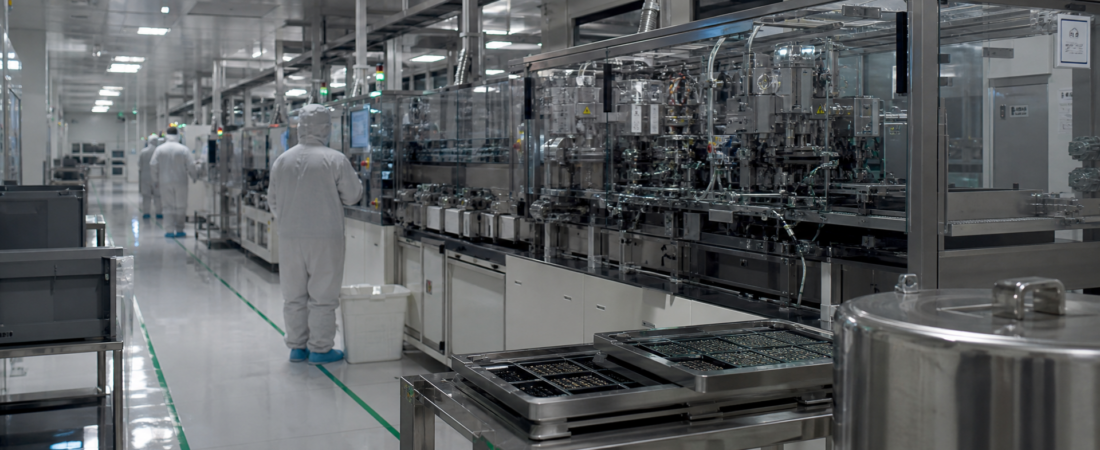
Executive Summary
According to the available source information, TSMC is reportedly targeting a 22% increase in 2nm capacity to 110,000 wafers per month and an increase of more than 16% in 3nm capacity to 210,000 wafers per month by mid-2027. The same report also points to a plan to double CoWoS advanced packaging capacity by 2028.
If accurate, that combination matters well beyond a routine foundry expansion update. Leading-edge logic and advanced packaging now sit at the core of the AI hardware stack. High-performance AI accelerators depend not only on access to advanced process nodes, but also on packaging technologies capable of integrating compute dies and high-bandwidth memory at scale. In practice, logic capacity and packaging capacity increasingly need to expand together.
For Asia’s technology landscape, the report reinforces a broader strategic reality: a large share of the world’s AI-enabling semiconductor manufacturing remains closely tied to Taiwan’s ecosystem. That concentration continues to shape supply-chain resilience, geopolitical risk, and the pace at which global AI infrastructure can actually be built.
Watch the Short Brief
Watch this short visual briefing for the key strategic implications behind the story.
Key Developments
According to the report summary, TSMC’s reported targets include three headline capacity goals:
– 2nm capacity rising by roughly 22% to 110,000 wafers per month by mid-2027.
– 3nm capacity increasing by more than 16% to 210,000 wafers per month by mid-2027.
– CoWoS advanced packaging capacity doubling by 2028.
Those figures, if realized, would represent a meaningful expansion across both wafer fabrication and advanced packaging. That is important because advanced AI chips increasingly require both scarce leading-edge silicon and scarce packaging capacity. A shortage in either layer can constrain final shipments.
The available source information does not provide additional detail on customer allocation, capex, fab-by-fab construction schedules, or the geographic split of the new capacity. It also does not establish how the added output would be distributed across end markets such as AI accelerators, smartphones, PCs, or data-center processors. As a result, the reported targets are best treated as capacity intentions rather than a complete operational roadmap.
Even so, the scale and timing of the reported goals are strategically significant. Mid-2027 for leading-edge logic and 2028 for CoWoS suggest that TSMC is planning against a multi-year demand horizon rather than a short-lived spike.
Strategic Analysis
The most important implication of the reported roadmap is that AI supply constraints should no longer be viewed only through the lens of transistor scaling. Packaging has become a strategic chokepoint.
For much of the semiconductor industry’s history, the main question was how quickly foundries could add advanced wafer capacity. In the AI cycle, that is no longer sufficient. Advanced accelerators depend on tightly integrated packaging architectures that connect high-performance logic with large pools of memory. CoWoS has therefore become one of the physical bottlenecks in the AI compute supply chain. The report’s emphasis on doubling CoWoS capacity by 2028 may indicate that TSMC sees packaging as a constraint that must be expanded alongside 2nm and 3nm output, not after it.
That matters for the broader AI buildout. Even where demand for high-end accelerators remains strong, supply can still be capped if packaging ramps more slowly than logic. One implication is that investors and industry participants should watch packaging availability as closely as wafer starts when assessing future AI server deployment.
A second implication is that TSMC appears, at least according to the report, to be planning with confidence in sustained advanced-node demand. Capacity additions at 2nm and 3nm are not short-cycle decisions. They require lengthy equipment procurement, process qualification, talent deployment, and ecosystem coordination. A reported push of this scale could suggest that TSMC expects durable demand visibility from customers building next-generation compute products, including AI-oriented silicon.
That interpretation should still be handled carefully. Capacity plans do not guarantee full utilization, and reported targets are not the same as completed ramp execution. But as a strategic signal, the roadmap points to expectations of continued pressure on advanced manufacturing capacity rather than an imminent normalization.
A third implication is geographic and highly relevant for Asia. The source summary itself does not specify where each tranche of new capacity will be installed. However, in strategic terms, any major TSMC expansion inevitably feeds into the question of concentration risk. Taiwan remains the center of the company’s most advanced manufacturing ecosystem, supported by dense supplier networks, engineering talent, and process learning accumulated over years. That ecosystem advantage is one reason TSMC remains so central to the global semiconductor chain.
For governments and customers seeking resilience, the key issue is not simply whether nominal capacity rises, but where that capacity sits and how quickly it becomes operational. Even without more detailed location data in the current source package, the reported expansion underscores how much of the AI era’s manufacturing foundation continues to depend on a limited set of highly specialized production clusters in Asia.
A fourth implication is competitive. The report does not provide direct comparisons with rival foundries, and the available information should not be stretched into unsupported market-share claims. Still, the combination of aggressive node expansion and a planned packaging ramp highlights the scale of execution required to compete at the top end of the foundry market. It is one thing to add advanced logic capacity. It is another to expand the packaging layer needed to convert wafers into deployable AI processors. TSMC’s reported roadmap suggests it is attempting to reinforce both layers simultaneously.
That dual expansion matters because the foundry competitive contest is no longer defined only by transistor leadership. The ability to coordinate front-end process technology with back-end advanced packaging increasingly shapes which suppliers can support hyperscale AI demand at volume.
Finally, the reported roadmap can be read as a practical indicator of how much AI infrastructure the industry may be able to absorb over the next two years. Public enthusiasm around AI often runs ahead of physical manufacturing constraints. Capacity announcements are therefore useful because they anchor the conversation in production reality. If the reported targets are met on schedule, they could help ease one part of the supply bottleneck in advanced AI hardware. If execution slips, supply tightness could persist even if end-market demand remains robust.
Investor Takeaway
The reported expansion plan is most useful as a framework for monitoring the next phase of AI semiconductor scaling.
First, investors should track whether future disclosures and industry checks show progress toward the reported mid-2027 targets for 2nm and 3nm. The critical question is not only whether nominal capacity rises, but whether yield, mix, and customer qualification allow that capacity to translate into commercially meaningful output.
Second, CoWoS deserves at least as much attention as leading-edge wafer capacity. In the current AI cycle, packaging is not a secondary detail. It may be one of the main determinants of how quickly AI accelerator supply constraints ease. If packaging growth lags, more wafer capacity alone may not resolve shipment bottlenecks.
Third, Asia remains central to the investment case around AI infrastructure and semiconductor supply chains. The concentration of advanced manufacturing capability in Taiwan continues to create both strategic leverage and geopolitical sensitivity. Any sign of diversification, delay, or operational friction around advanced-node and packaging expansion could ripple across the broader AI hardware ecosystem.
Fourth, investors should be cautious about reading the reported targets as automatic proof of demand quality. A capacity roadmap can indicate confidence, but it does not by itself reveal customer concentration, pricing discipline, or end-market durability. The next layer of analysis will depend on how much of this reported expansion is supported by sustained orders rather than cyclical overbooking or short-term urgency.
Overall, the report points to a simple but important conclusion: in the AI era, semiconductor leadership depends on scaling both advanced logic and advanced packaging together. If TSMC executes on the reported roadmap, it could reinforce its position at the center of the global AI supply chain. For TechPowerAsia readers, the larger takeaway is that Asia’s semiconductor infrastructure remains one of the decisive foundations of AI growth, and capacity expansion timelines are becoming one of the clearest signals of how fast that growth can actually materialize.