Executive Summary
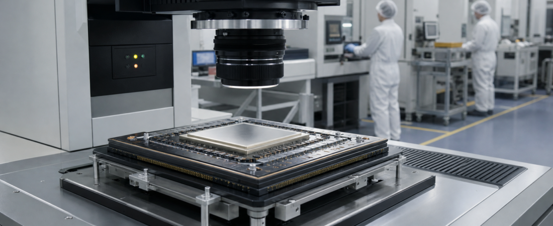
According to the available source information, TSMC Vice President Ho Chun said the company has reached a 98% yield rate for certain CoWoS advanced packaging products used in AI-related chips. The reported figure applies to products using a 5.5x reticle size, indicating progress in a package format associated with large AI processors.
That matters because advanced packaging has become one of the most important constraints in the AI semiconductor stack. Leading AI chips increasingly depend not only on advanced logic fabrication, but also on the ability to assemble large, complex packages that combine compute dies, memory, and interconnect structures at high reliability. In that environment, packaging yield can influence how much usable AI silicon actually reaches the market.
For Asia’s technology supply chain, the report also reinforces a broader point: Taiwan’s role in AI hardware is not limited to wafer fabrication. Packaging capability is emerging as a strategic control point in its own right. If the reported yield level is sustained at scale, it could strengthen TSMC’s position in a part of the semiconductor value chain that is becoming more central to AI infrastructure deployment.
Watch the Short Brief
Watch this short visual briefing for the key strategic implications behind the story.
Key Developments
According to the report, TSMC Vice President Ho Chun stated that the company has achieved a 98% yield rate for certain CoWoS products tied to AI applications.
The reported yield applies only to specific products rather than to all CoWoS output. That distinction matters. Investors and industry observers should avoid treating the figure as a blanket measure of TSMC’s entire advanced packaging portfolio.
The source information also indicates that the reported products use a 5.5x reticle size. While the available details are limited, that suggests TSMC is discussing a larger-format packaging configuration relevant to increasingly complex AI chip designs.
CoWoS, or Chip-on-Wafer-on-Substrate, is one of TSMC’s core advanced packaging technologies and is widely associated with AI accelerator production. In practical terms, it enables multiple silicon components to be integrated into a single high-performance package, which is particularly important for AI systems that require close coupling between compute and memory.
The report did not identify the specific customers, chip models, production volumes, or the time period over which the reported yield was achieved. It also did not provide updated capacity targets, pricing implications, or a company-wide view of CoWoS performance.
Strategic Analysis
The most important takeaway is not the headline number by itself, but what it says about where the AI hardware bottleneck now sits. For much of the last decade, semiconductor leadership was commonly discussed in terms of leading-edge process nodes. That remains important. But in AI, manufacturing success increasingly depends on what happens after the wafers are made.
Large AI accelerators are no longer simple monolithic products in every case. They increasingly rely on advanced packaging to bring together multiple dies, memory stacks, and dense interconnects into a single module. That means the packaging step can determine whether expensive leading-edge silicon becomes a saleable product or a constrained asset stuck in the back end of the manufacturing chain.
From that perspective, a reported 98% yield for certain CoWoS AI products could be strategically meaningful if it proves repeatable and scalable. High yield at the packaging stage can improve effective output without requiring an equivalent increase in front-end wafer starts. In other words, the industry may get more usable AI accelerators from the same underlying silicon input if packaging execution improves.
That is particularly relevant in an environment where AI demand continues to pull on several tightly linked supply chains at once: advanced logic, high-bandwidth memory, substrates, test, and packaging. The value of an incremental yield gain in packaging is magnified because each completed package already contains costly components and significant manufacturing time. Packaging efficiency therefore has implications not just for throughput, but also for capital productivity across the broader AI hardware stack.
The 5.5x reticle detail, while only lightly described in the available source information, adds another layer of significance. Larger and more complex package formats are generally harder to manufacture consistently than smaller, simpler ones. If TSMC is reporting very high yields on a larger AI-oriented CoWoS configuration, one implication is that the company may be improving process control in a part of the workflow that many outside observers increasingly view as a critical chokepoint.
That does not mean the broader CoWoS constraint is solved. A high reported yield on certain products does not automatically translate into unconstrained supply across all AI accelerators, all customers, or all package types. Capacity, equipment availability, qualification cycles, and mix complexity still matter. A strong yield figure can improve output economics and execution, but it does not by itself answer the bigger question of whether demand is being met across the full market.
Still, the report fits a larger structural narrative that matters for TechPowerAsia readers. Taiwan’s semiconductor importance in the AI era is often framed around foundry leadership. Yet the packaging layer is becoming nearly as strategically significant for some of the industry’s highest-value products. If TSMC continues to execute well in advanced packaging, Taiwan’s role in the global AI supply chain may deepen not only at the fabrication level, but also in the final assembly architecture that turns chips into deployable accelerators.
That concentration has two different implications. On one hand, it can reinforce TSMC’s competitive strength and support tighter customer alignment around its manufacturing ecosystem. On the other, it underscores how much of the global AI hardware pipeline remains dependent on specialized capabilities concentrated in Asia, especially in Taiwan. For governments, hyperscalers, and semiconductor customers seeking supply-chain resilience, that concentration remains a strategic issue even if operational performance improves.
Competitive implications should also be framed carefully. The reported milestone could suggest that TSMC is extending its lead in a technically demanding segment of semiconductor manufacturing. But the available information does not provide direct comparative data versus other packaging providers or foundries. The safer conclusion is that strong execution in CoWoS may strengthen TSMC’s position at a moment when advanced packaging has become more central to AI chip availability.
Investor Takeaway
The reported 98% CoWoS yield should be read as an important operational signal, not as a standalone conclusion about the AI chip market.
First, investors should monitor whether TSMC provides further disclosure through formal company channels. The key issue is not simply whether the number was reported, but whether TSMC elaborates on the scope: which product classes it covers, whether the performance is sustained in volume production, and how broadly it applies across the CoWoS portfolio.
Second, capacity still matters as much as yield. Even excellent yield on certain products will have limited market impact if advanced packaging throughput remains tight. Future commentary on CoWoS expansion, utilization, and customer demand will be more important than the headline figure alone in assessing whether supply constraints are easing.
Third, downstream customer signals are worth watching. If packaging yield and execution are materially improving, one possible result would be better delivery visibility for AI accelerator programs that depend on TSMC’s advanced packaging stack. Over time, that could affect lead times, deployment schedules, and revenue timing across parts of the AI infrastructure ecosystem.
Fourth, the report reinforces the strategic value of packaging within Asia’s semiconductor landscape. For readers tracking capital flows and supply-chain control points, this is a reminder that the AI race is not only about compute architecture or leading-edge lithography. It is also about who can assemble increasingly complex systems at industrial scale.
Finally, caution remains warranted. The available source information is narrow, and the reported yield figure applies to certain AI-related CoWoS products rather than the entire business. If confirmed and sustained, it could mark a meaningful step for TSMC’s packaging execution. But broader conclusions about total market supply, margin impact, or competitor displacement will require more disclosure than is currently available.